User Manual
Page 1
R P/I-P55TVP4 Pentium Motherboard USER'S MANUAL
R P/I-P55TVP4 Pentium Motherboard USER'S MANUAL

User Manual
Page 2
... are both printed on the board itself. All rights reserved. Product Name: ASUS P/I-P55TVP4 Manual Revision: 1.52 Release Date: December 1996 II ASUS P/I-P55TVP4 User's Manual Product names appearing in this manual "as ASUS) except documentation kept by the third digit in the manual revision number. USER'S NOTICE No part of this product, including the product and software may...
... are both printed on the board itself. All rights reserved. Product Name: ASUS P/I-P55TVP4 Manual Revision: 1.52 Release Date: December 1996 II ASUS P/I-P55TVP4 User's Manual Product names appearing in this manual "as ASUS) except documentation kept by the third digit in the manual revision number. USER'S NOTICE No part of this product, including the product and software may...

User Manual
Page 3
...: Fax: 886-2-895-9254 BBS: 886-2-896-4667 Email: tsd@asus.com.tw WWW: http://www.asus.com.tw/ Gopher: gopher.asus.com.tw FTP: ftp.asus.com.tw/pub/ASUS ASUS COMPUTER INTERNATIONAL Marketing Info: Address: 721 Charcot Avenue, San Jose, CA...asus.com.tw Technical Support: BBS: 1-408-474-0555 Email: tsd-usa@asus.com.tw ASUS COMPUTER GmbH Marketing Info: Address: Harkort Str. 25, 40880 Ratingen, BRD, Germany Telephone: 49-2102-445011 Fax: 49-2102-442066 Email: info-ger@asus.com.tw Technical Support: BBS: 49-2102-448690 Email: tsd-ger@asus.com.tw ASUS P/I-P55TVP4 User's Manual...
...: Fax: 886-2-895-9254 BBS: 886-2-896-4667 Email: tsd@asus.com.tw WWW: http://www.asus.com.tw/ Gopher: gopher.asus.com.tw FTP: ftp.asus.com.tw/pub/ASUS ASUS COMPUTER INTERNATIONAL Marketing Info: Address: 721 Charcot Avenue, San Jose, CA...asus.com.tw Technical Support: BBS: 1-408-474-0555 Email: tsd-usa@asus.com.tw ASUS COMPUTER GmbH Marketing Info: Address: Harkort Str. 25, 40880 Ratingen, BRD, Germany Telephone: 49-2102-445011 Fax: 49-2102-442066 Email: info-ger@asus.com.tw Technical Support: BBS: 49-2102-448690 Email: tsd-ger@asus.com.tw ASUS P/I-P55TVP4 User's Manual...
User Manual
Page 4
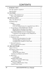
...DRAM Memory Installation Procedures 12 SDRAM Memory Installation Procedures 13 Static RAM (SRAM) for Level 2 (External) Cache 14 Compatible Cache Modules for this manual is organized 1 Item Checklist 1 II. BIOS Setup 29 Load Defaults 30 Standard CMOS Setup 30 Details of Standard CMOS Setup 31 BIOS Features ...Setup 34 Details of BIOS Features Setup 34 Chipset Features Setup 37 IV ASUS P/I . CONTENTS I -P55TVP4 User's Manual INTRODUCTION 1 How this Motherboard 14 3. External Connectors 19 Power Connection Procedures 25 IV.
...DRAM Memory Installation Procedures 12 SDRAM Memory Installation Procedures 13 Static RAM (SRAM) for Level 2 (External) Cache 14 Compatible Cache Modules for this manual is organized 1 Item Checklist 1 II. BIOS Setup 29 Load Defaults 30 Standard CMOS Setup 30 Details of Standard CMOS Setup 31 BIOS Features ...Setup 34 Details of BIOS Features Setup 34 Chipset Features Setup 37 IV ASUS P/I . CONTENTS I -P55TVP4 User's Manual INTRODUCTION 1 How this Motherboard 14 3. External Connectors 19 Power Connection Procedures 25 IV.

User Manual
Page 5
...) IX. DESKTOP MANAGEMENT 49 Desktop Management Interface (DMI 49 Introducing the ASUS DMI Configuration Utility 49 System Requirements 49 Using the ASUS DMI Configuration Utility 50 Notes 50 VI. Windows 95 Audio Software (with optional ASUS I -P55TVP4 User's Manual V ASUS I-A16C Audio Card 57 ASUS I-A16C Audio Features 57 Unpacking and Handling Precautions 57 Layout and Connectors...
...) IX. DESKTOP MANAGEMENT 49 Desktop Management Interface (DMI 49 Introducing the ASUS DMI Configuration Utility 49 System Requirements 49 Using the ASUS DMI Configuration Utility 50 Notes 50 VI. Windows 95 Audio Software (with optional ASUS I -P55TVP4 User's Manual V ASUS I-A16C Audio Card 57 ASUS I-A16C Audio Features 57 Unpacking and Handling Precautions 57 Layout and Connectors...

User Manual
Page 6
... could void the user's authority to Part 15 of the FCC Rules. These limits are designed to assure compliance with FCC Rules Part 15. VI ASUS P/I-P55TVP4 User's Manual FCC & DOC COMPLIANCE Federal Communications Commission Statement This device complies with FCC regulations.
... could void the user's authority to Part 15 of the FCC Rules. These limits are designed to assure compliance with FCC Rules Part 15. VI ASUS P/I-P55TVP4 User's Manual FCC & DOC COMPLIANCE Federal Communications Commission Statement This device complies with FCC regulations.

User Manual
Page 7
... Setup: BIOS software setup information. INTRODUCTION How this product III. Installation: Instructions on setting up the motherboard. INTRODUCTION (Manual / Checklist) I -A16C bundle) Item Checklist Please check that your retailer. √ The ASUS P/I-P55TVP4 motherboard √ 2 serial port ribbon cables attached to a mounting bracket √ 1 parallel ribbon cable with mounting bracket √ 1 IDE ribbon...
... Setup: BIOS software setup information. INTRODUCTION How this product III. Installation: Instructions on setting up the motherboard. INTRODUCTION (Manual / Checklist) I -A16C bundle) Item Checklist Please check that your retailer. √ The ASUS P/I-P55TVP4 motherboard √ 2 serial port ribbon cables attached to a mounting bracket √ 1 parallel ribbon cable with mounting bracket √ 1 IDE ribbon...

User Manual
Page 8
...; Super Multi-I/O: Provides two high-speed UART compatible serial ports and one parallel port with I -P55TVP4 User's Manual Upgrades are also supported without an external card. BIOS supports IDE CD-ROM boot-up. 2 ASUS P/I /O subsystems. • Desktop Management Interface (DMI): Supports DMI through a Synchronous SRAM cache ...can also be directed from COM2 to 256KB or 512KB. Two floppy drives of either a standard PCI card or the ASUS MediaBus Card. • ASUS MediaBus Rev 2.0: Features an expansion slot extension shared with BIOS that supports four IDE devices in 0KB, 256KB, or ...
...; Super Multi-I/O: Provides two high-speed UART compatible serial ports and one parallel port with I -P55TVP4 User's Manual Upgrades are also supported without an external card. BIOS supports IDE CD-ROM boot-up. 2 ASUS P/I /O subsystems. • Desktop Management Interface (DMI): Supports DMI through a Synchronous SRAM cache ...can also be directed from COM2 to 256KB or 512KB. Two floppy drives of either a standard PCI card or the ASUS MediaBus Card. • ASUS MediaBus Rev 2.0: Features an expansion slot extension shared with BIOS that supports four IDE devices in 0KB, 256KB, or ...
User Manual
Page 9
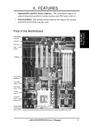
... 2.0 72-pin SIMM Sockets Intel's 430VX PCIset CPU ZIF Socket 7 L2 Upgrade Cache Expansion Slot Onboard 256KB/ 512KB Pipelined Burst L2 Cache ASUS P/I /O 1 DIMM Slot II. FEATURES • Optional IrDA and PS/2 Mouse Connector: This motherboard supports an optional infrared port module for wireless interface and a ...PS/2 mouse cable set. • NCR SCSI BIOS: This motherboard has firmware that supports the optional ASUS PCI-SC200 SCSI controller cards. II. FEATURES (Parts of the Motherboard Programmable Flash ROM 3 ISA Slots 3 PCI Slots Super Multi...
... 2.0 72-pin SIMM Sockets Intel's 430VX PCIset CPU ZIF Socket 7 L2 Upgrade Cache Expansion Slot Onboard 256KB/ 512KB Pipelined Burst L2 Cache ASUS P/I /O 1 DIMM Slot II. FEATURES • Optional IrDA and PS/2 Mouse Connector: This motherboard supports an optional infrared port module for wireless interface and a ...PS/2 mouse cable set. • NCR SCSI BIOS: This motherboard has firmware that supports the optional ASUS PCI-SC200 SCSI controller cards. II. FEATURES (Parts of the Motherboard Programmable Flash ROM 3 ISA Slots 3 PCI Slots Super Multi...
User Manual
Page 10
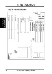
...4 (Bank 1) SIMM Slot 3 (Bank 1) SIMM Slot 2 (Bank 0) SIMM Slot 1 (Bank 0) Floppy Drives Secondary IDE Primary IDE PCI Slot 1 Super Multi I/O PCI Slot 2 Multi I -P55TVP4 User's Manual Case Conn (CON 1) Vio/Vcore JP22 JP21 JP20 JP19 JP18 JP17 JP16 BUS Ratio IDE LED Clear CMOS JP7 256/512KB OnBoard L2 Cache... 4 ASUS P/I /O Boot Program JP9 JP10 PCI Slot 3 PCI Slot 4 / MediaBus 2.0 ISA Slot 1 ISA Slot 2 ISA Slot 3 III. INSTALLATION Map of Board) BUS ...
...4 (Bank 1) SIMM Slot 3 (Bank 1) SIMM Slot 2 (Bank 0) SIMM Slot 1 (Bank 0) Floppy Drives Secondary IDE Primary IDE PCI Slot 1 Super Multi I/O PCI Slot 2 Multi I -P55TVP4 User's Manual Case Conn (CON 1) Vio/Vcore JP22 JP21 JP20 JP19 JP18 JP17 JP16 BUS Ratio IDE LED Clear CMOS JP7 256/512KB OnBoard L2 Cache... 4 ASUS P/I /O Boot Program JP9 JP10 PCI Slot 3 PCI Slot 4 / MediaBus 2.0 ISA Slot 1 ISA Slot 2 ISA Slot 3 III. INSTALLATION Map of Board) BUS ...

User Manual
Page 11
... SMI Switch Lead (2-pins) p. 23 Reset Switch Lead (2-pins) p. 23 Keyboard Lock Switch Lead (5-pins) p. 23 Speaker Output Connector (4-pins) p. 24 Infrared Port Module Connector ASUS P/I-P55TVP4 User's Manual 5 III.
... SMI Switch Lead (2-pins) p. 23 Reset Switch Lead (2-pins) p. 23 Keyboard Lock Switch Lead (5-pins) p. 23 Speaker Output Connector (4-pins) p. 24 Infrared Port Module Connector ASUS P/I-P55TVP4 User's Manual 5 III.
User Manual
Page 12
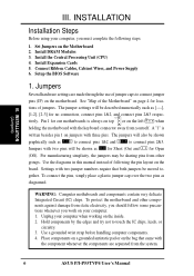
... 4. Install Expansion Cards 5. Install DRAM Modules 3. Setup the BIOS Software 1. See "Map of following steps: 1. Use the diagrams in this manual instead of the Motherboard" on the inside. 2. To connect the pins, simply place a plastic jumper cap over the two pins as [----], [1-2],...antistatic pad or on the bag that both jumpers be sharing pins from other components against damage from the system. 6 ASUS P/I-P55TVP4 User's Manual Pin 1 for our motherboards is written besides pin 1 on the left when holding the motherboard with the component whenever the...
... 4. Install Expansion Cards 5. Install DRAM Modules 3. Setup the BIOS Software 1. See "Map of following steps: 1. Use the diagrams in this manual instead of the Motherboard" on the inside. 2. To connect the pins, simply place a plastic jumper cap over the two pins as [----], [1-2],...antistatic pad or on the bag that both jumpers be sharing pins from other components against damage from the system. 6 ASUS P/I-P55TVP4 User's Manual Pin 1 for our motherboards is written besides pin 1 on the left when holding the motherboard with the component whenever the...

User Manual
Page 13
...Jumper Settings 1. Selections Enable Disable JP9 [1-2] (Default) [2-3] JP9 1 2 3 Enable (Default) 1 2 3 Disabled Multi I -P55TVP4 User's Manual 7 This is required only if prompted by the Flash Memory Writer Utility as shown in the Enabled position. Flash ROM Boot Block ...can selectively disable each onboard Multi-I /O card. Programming Disabled Enabled JP10 [1-2] (Default) [2-3] JP10 1 2 3 Disabled / Protected (Default) 1 2 3 Enabled Boot Block Programming (Disable / Enable) ASUS P/I /O Setting (Enable / Disable) JP10 JP9 2. III. INSTALLATION (Jumpers) III.
...Jumper Settings 1. Selections Enable Disable JP9 [1-2] (Default) [2-3] JP9 1 2 3 Enable (Default) 1 2 3 Disabled Multi I -P55TVP4 User's Manual 7 This is required only if prompted by the Flash Memory Writer Utility as shown in the Enabled position. Flash ROM Boot Block ...can selectively disable each onboard Multi-I /O card. Programming Disabled Enabled JP10 [1-2] (Default) [2-3] JP10 1 2 3 Disabled / Protected (Default) 1 2 3 Enabled Boot Block Programming (Disable / Enable) ASUS P/I /O Setting (Enable / Disable) JP10 JP9 2. III. INSTALLATION (Jumpers) III.
User Manual
Page 14
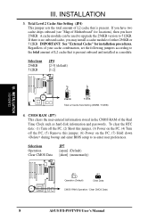
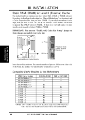
... 256KB or 512KB. Selections Operation Clear CMOS Data JP7 [open] (Default) [short] (momentarily) JP7 Operation (Default) JP7 Clear Data CMOS RAM (Operation / Clear CMOS Data) 8 ASUS P/I-P55TVP4 User's Manual III. If you may install a cache module of L2 cache that is present. If there is no onboard cache, you have 256KB.
... 256KB or 512KB. Selections Operation Clear CMOS Data JP7 [open] (Default) [short] (momentarily) JP7 Operation (Default) JP7 Clear Data CMOS RAM (Operation / Clear CMOS Data) 8 ASUS P/I-P55TVP4 User's Manual III. If you may install a cache module of L2 cache that is present. If there is no onboard cache, you have 256KB.
User Manual
Page 15
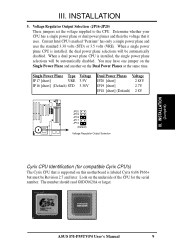
.... Voltage Regulator Output Selection (JP16-JP20) These jumpers set the voltage supplied to the CPU. Look on the Dual Power Planes at the same time. ASUS P/I-P55TVP4 User's Manual 9 INSTALLATION 5.
.... Voltage Regulator Output Selection (JP16-JP20) These jumpers set the voltage supplied to the CPU. Look on the Dual Power Planes at the same time. ASUS P/I-P55TVP4 User's Manual 9 INSTALLATION 5.
User Manual
Page 16
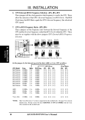
... clock generator what frequency to send to BUS Frequency Ratio (JP5, JP6) These jumpers set together with the Cyrix 166+ installed on this motherboard. 10 ASUS P/I-P55TVP4 User's Manual The BUS Clock times the BUS Ratio equals the CPU's Internal frequency (the advertised CPU speed). 7.
... clock generator what frequency to send to BUS Frequency Ratio (JP5, JP6) These jumpers set together with the Cyrix 166+ installed on this motherboard. 10 ASUS P/I-P55TVP4 User's Manual The BUS Clock times the BUS Ratio equals the CPU's Internal frequency (the advertised CPU speed). 7.
User Manual
Page 17
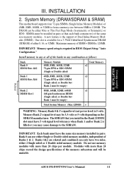
...: Memory Bank 0 & 1's signal level (not power level) is the support of either 60ns or 70ns Fast Page Mode (Asymmetric or Symmetric) or EDO. Related ASUS P/I-P55TVP4 User's Manual 11 IMPORTANT: Each bank must be installed in the Bank 2 DIMM slot must be 3.3 volts or 5 volts depending on the SDRAM manufacturer. SIMMs must have...
...: Memory Bank 0 & 1's signal level (not power level) is the support of either 60ns or 70ns Fast Page Mode (Asymmetric or Symmetric) or EDO. Related ASUS P/I-P55TVP4 User's Manual 11 IMPORTANT: Each bank must be installed in the Bank 2 DIMM slot must be 3.3 volts or 5 volts depending on the SDRAM manufacturer. SIMMs must have...

User Manual
Page 18
... sides and the "Metal Clips" should snap on one end of the SIMM slots which requires the "Notched End" of the "Metal Clips". 12 ASUS P/I-P55TVP4 User's Manual To release the memory module, squeeze both "Metal Clips" outwards and rock the module out of the SIMM memory modules. 1234 DRAM Memory Module Example...
... sides and the "Metal Clips" should snap on one end of the SIMM slots which requires the "Notched End" of the "Metal Clips". 12 ASUS P/I-P55TVP4 User's Manual To release the memory module, squeeze both "Metal Clips" outwards and rock the module out of the SIMM memory modules. 1234 DRAM Memory Module Example...
User Manual
Page 19
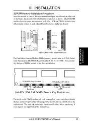
... DIMM slot on both sides. SDRAM DIMM modules have different pint contact on each side and therefore have the same pin contact on the motherboard. ASUS P/I-P55TVP4 User's Manual 13 INSTALLATION SDRAM Memory Installation Procedures: Insert the module as shown. III.
... DIMM slot on both sides. SDRAM DIMM modules have different pint contact on each side and therefore have the same pin contact on the motherboard. ASUS P/I-P55TVP4 User's Manual 13 INSTALLATION SDRAM Memory Installation Procedures: Insert the module as shown. III.
User Manual
Page 20
... 512KB ---------Yes Yes ---------Yes Yes Yes Yes 0KB to 256/512KB Yes ---------Yes Yes Yes Yes * NOTE: ASUS CM1 Rev 3.0 has two TAG SRAM's to comply with the onboard TAG SRAM. 14 ASUS P/I-P55TVP4 User's Manual INSTALLATION (External Cache) 42 Pins 38 Pins Pipelined Burst Cache Module Example Pipelined Burst Cache Module Insert the...
... 512KB ---------Yes Yes ---------Yes Yes Yes Yes 0KB to 256/512KB Yes ---------Yes Yes Yes Yes * NOTE: ASUS CM1 Rev 3.0 has two TAG SRAM's to comply with the onboard TAG SRAM. 14 ASUS P/I-P55TVP4 User's Manual INSTALLATION (External Cache) 42 Pins 38 Pins Pipelined Burst Cache Module Example Pipelined Burst Cache Module Insert the...


