Service Manual
Page 1
... PIONEER ELECTRONIC CORPORATION 4-1, Meguro 1-Chome, Meguro-ku, Tokyo 153-8654, Japan PIONEER ELECTRONICS SERVICE, INC. Haven 1087, Keetberglaan 1, 9120 Melsele, Belgium PIONEER ELECTRONICS ASIACENTRE PTE. THIS MANUAL IS APPLICABLE TO THE FOLLOWING MODEL(S) AND TYPE(S). P.O. Box 1760, Long Beach, CA 90801-1760, U.S.A. ZZM APR. 1998 Printed in Japan Type Model DV-606D Power Requirement Remarks KU AC120V KC AC120V CONTENTS 1. PIONEER ELECTRONIC (EUROPE) N.V. ADJUSTMENT 16 5. DVD PLAYER DV-606D...
... PIONEER ELECTRONIC CORPORATION 4-1, Meguro 1-Chome, Meguro-ku, Tokyo 153-8654, Japan PIONEER ELECTRONICS SERVICE, INC. Haven 1087, Keetberglaan 1, 9120 Melsele, Belgium PIONEER ELECTRONICS ASIACENTRE PTE. THIS MANUAL IS APPLICABLE TO THE FOLLOWING MODEL(S) AND TYPE(S). P.O. Box 1760, Long Beach, CA 90801-1760, U.S.A. ZZM APR. 1998 Printed in Japan Type Model DV-606D Power Requirement Remarks KU AC120V KC AC120V CONTENTS 1. PIONEER ELECTRONIC (EUROPE) N.V. ADJUSTMENT 16 5. DVD PLAYER DV-606D...
Service Manual
Page 2
... unavailable because they are 2 effective digits (any digit apart from 0), such as in our Master Spare Parts List. PCB CONNECTION DIAGRAM". 2 DV-606D 1. The mark found on "7 EXPLOEDE VIEWS". Ex.1 When there are not in high precision metal film resistors). 5.62k 562 x 101 5621 RN1/4PC 5 6 2 1 F Reference Nos. DVDM CN804) VDA1646 VNA1903 VKP2157 Not used VNE2085 VNE2085 No.10 P6...
... unavailable because they are 2 effective digits (any digit apart from 0), such as in our Master Spare Parts List. PCB CONNECTION DIAGRAM". 2 DV-606D 1. The mark found on "7 EXPLOEDE VIEWS". Ex.1 When there are not in high precision metal film resistors). 5.62k 562 x 101 5621 RN1/4PC 5 6 2 1 F Reference Nos. DVDM CN804) VDA1646 VNA1903 VKP2157 Not used VNE2085 VNE2085 No.10 P6...
Service Manual
Page 3
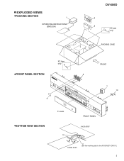
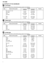
EXPLODED VIEWS ÷PACKING SECTION 1 OPERATING INSTRUCTIONS (ENGLISH) DV-606D 43 2 6 KC type 5 only PACKING CASE ÷FRONT PANEL SECTION KC type only 5 9 FRONT 8 7 10 ÷BOTTOM VIEW SECTION FL Lens FRONT PANEL AVJB ASSY 12 CN803 CN804 CN802 DVDM ASSY CNC1N01102 CN104 11 (Set the marking side to the AVJB ASSY CN101.) 3
EXPLODED VIEWS ÷PACKING SECTION 1 OPERATING INSTRUCTIONS (ENGLISH) DV-606D 43 2 6 KC type 5 only PACKING CASE ÷FRONT PANEL SECTION KC type only 5 9 FRONT 8 7 10 ÷BOTTOM VIEW SECTION FL Lens FRONT PANEL AVJB ASSY 12 CN803 CN804 CN802 DVDM ASSY CNC1N01102 CN104 11 (Set the marking side to the AVJB ASSY CN101.) 3
Service Manual
Page 4
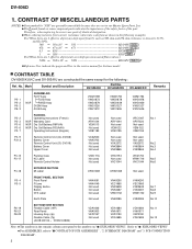
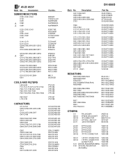
DV-606D CONTRAST OF PCB ASSEMBLIES FLKB ASSY VWG1878 and VWG1873 are constructed the same except for the following : Mark Symbol and Description Part No. VWS1326 VWS1327 IC602 IC6003 IC801 F9141,F9921 L9143,L9930,L9931 Not used VYW1559 MB86371A Not used Not used PDK026C VYW1546 MB86371 VTF1096 ...Mark Symbol and Description Part No. VWG1873 VWG1878 Q101,Q104,Q106-Q108 D101-D108 R101-R108 R124 R126,R606 Not used Not used Not used RS1/10S0R0J Not used PDTC124EK SLP4118C51H RS1/10S331J Not used RS1/10S0R0J R127 R137 S101 RS1/10S0R0J Not used Not used RS1/16S271J RS1/...
DV-606D CONTRAST OF PCB ASSEMBLIES FLKB ASSY VWG1878 and VWG1873 are constructed the same except for the following : Mark Symbol and Description Part No. VWS1326 VWS1327 IC602 IC6003 IC801 F9141,F9921 L9143,L9930,L9931 Not used VYW1559 MB86371A Not used Not used PDK026C VYW1546 MB86371 VTF1096 ...Mark Symbol and Description Part No. VWG1873 VWG1878 Q101,Q104,Q106-Q108 D101-D108 R101-R108 R124 R126,R606 Not used Not used Not used RS1/10S0R0J Not used PDTC124EK SLP4118C51H RS1/10S331J Not used RS1/10S0R0J R127 R137 S101 RS1/10S0R0J Not used Not used RS1/16S271J RS1/...
Service Manual
Page 5
...CCSQCH330J50 CCSQCH330J50 CCSQCH331J50 CCSQCH331J50 CCSQCH331J50 CCSQCH470J50 CCSQCH470J50 CEAL101M6R3 CEAT100M50 CEAT101M10 CEAT101M10 CEAT101M10 CEAT101M16 CEAT102M6R3 CEAT1R0M50 CEAT221M16 CEAT470M16 DV-606D Mark No. Description C407,C408,C572 C936,C956 C253,C254,C259,C260 C353,C453,C454,C559,C566...,C702,C751,C755,C756 C802,C852,C913,C914,C933,C934 C953,C954 C607,C657 VC131 (20pF) Part No. CEAT470M16 CEAT471M6R3 CEBA101M16 CFTYA104J50 CKSQYB103K50 CKSQYB104K25 CKSQYB105K10 CKSQYF103Z50 CKSQYF103Z50 CKSQYF103Z50 CKSQYF103Z50 CKSQYF103Z50 CKSQYF103Z50 CKSQYF103Z50 CKSQYF103Z50 CKSQYF103Z50...
...CCSQCH330J50 CCSQCH330J50 CCSQCH331J50 CCSQCH331J50 CCSQCH331J50 CCSQCH470J50 CCSQCH470J50 CEAL101M6R3 CEAT100M50 CEAT101M10 CEAT101M10 CEAT101M10 CEAT101M16 CEAT102M6R3 CEAT1R0M50 CEAT221M16 CEAT470M16 DV-606D Mark No. Description C407,C408,C572 C936,C956 C253,C254,C259,C260 C353,C453,C454,C559,C566...,C702,C751,C755,C756 C802,C852,C913,C914,C933,C934 C953,C954 C607,C657 VC131 (20pF) Part No. CEAT470M16 CEAT471M6R3 CEBA101M16 CFTYA104J50 CKSQYB103K50 CKSQYB104K25 CKSQYB105K10 CKSQYF103Z50 CKSQYF103Z50 CKSQYF103Z50 CKSQYF103Z50 CKSQYF103Z50 CKSQYF103Z50 CKSQYF103Z50 CKSQYF103Z50 CKSQYF103Z50...
Service Manual
Page 7
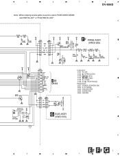
5 6 7 Note : When ordering service parts, be sure to refer to "EXPLODED VIEWS and PARTS LIST" or "PCB PARTS LIST". 8 DV-606D A 330 D202 SLP4118C51H 5.1CH MODE PWSB ASSY (VWG1939) D201 SLP9118C51H B AC1 AC2 H 2/3 CN105 FLKB ASSY S101 : FL OFF S102 : (OPEN/CLOSE) S103 : (REV) S104 : (FWD) S105 : (STOP) S106 : (PLAY/PAUSE) PWSB ASSY S201 : POWER (STANDBY/ON) S202 : 5.1CH MODE S203 : SUB WOOFER S204 : SURROUND S205 : CENTER C REMOTE RECEIVER UNIT G DILB ASSY (VWG1881) C112 0.1 R118 0 D G7 5 6 7 8
5 6 7 Note : When ordering service parts, be sure to refer to "EXPLODED VIEWS and PARTS LIST" or "PCB PARTS LIST". 8 DV-606D A 330 D202 SLP4118C51H 5.1CH MODE PWSB ASSY (VWG1939) D201 SLP9118C51H B AC1 AC2 H 2/3 CN105 FLKB ASSY S101 : FL OFF S102 : (OPEN/CLOSE) S103 : (REV) S104 : (FWD) S105 : (STOP) S106 : (PLAY/PAUSE) PWSB ASSY S201 : POWER (STANDBY/ON) S202 : 5.1CH MODE S203 : SUB WOOFER S204 : SURROUND S205 : CENTER C REMOTE RECEIVER UNIT G DILB ASSY (VWG1881) C112 0.1 R118 0 D G7 5 6 7 8
Service Manual
Page 8
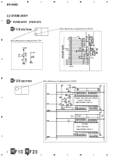
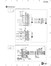
1 2 DV-606D 2.2 DVDM ASSY A DVDM ASSY (VWS1327) 1/3 SECTION ÷The differences of adjacencies to TP1 B 33K 22K PICKUP ASSY F9141 VTF1096 3 4 ÷The differences of adjacencies to CN102 (F) (F) (T) (F) (F) (T) CN102 VKN1445 L9143 (F) (T) (F) (T) L9143: QTL1011 2/3 SECTION ÷The differences of adjacencies to IC6003 C D 8 H F 1/3 H F 2/3 1 2 IC6003 VYW1546 R643 0 R642 10K R641 0 C606 0.1 IC602 PDK026C C607 0.1 3 4
1 2 DV-606D 2.2 DVDM ASSY A DVDM ASSY (VWS1327) 1/3 SECTION ÷The differences of adjacencies to TP1 B 33K 22K PICKUP ASSY F9141 VTF1096 3 4 ÷The differences of adjacencies to CN102 (F) (F) (T) (F) (F) (T) CN102 VKN1445 L9143 (F) (T) (F) (T) L9143: QTL1011 2/3 SECTION ÷The differences of adjacencies to IC6003 C D 8 H F 1/3 H F 2/3 1 2 IC6003 VYW1546 R643 0 R642 10K R641 0 C606 0.1 IC602 PDK026C C607 0.1 3 4
Service Manual
Page 9
... 105pin) (to IC701 20pin) (to IC701 19pin) (to IC804 16pin) (to IC804 17pin) (to IC804 18pin) ÷The differences of adjacencies to IC801 I F1/2 CN102 8 DV-606D A B C IC801 MB86371 R866 R865 R864 AV-1 R830 D H F 3/3 9 5 6 7 8
... 105pin) (to IC701 20pin) (to IC701 19pin) (to IC804 16pin) (to IC804 17pin) (to IC804 18pin) ÷The differences of adjacencies to IC801 I F1/2 CN102 8 DV-606D A B C IC801 MB86371 R866 R865 R864 AV-1 R830 D H F 3/3 9 5 6 7 8
Service Manual
Page 14
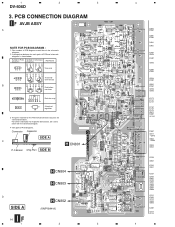
View point of PCB and schematic diagrams is shown below. A comparison between the main parts of PCB diagrams. Connector Capacitor SIDE A C P.C.Board Chip Part SIDE B H CN801 H CN804 H ...parts mounted on this PCB include all necessary parts for respective destinations, be sure to check with resistor B D G SD G S Field effect DGS transistor Resistor array 3-terminal regulator 3. 1 2 3 DV-606D 3. Symbol In PCB Diagrams Symbol In Schematic Diagrams B C EB C E Part Name BCE Transistor BCE B C EB C E Transistor with the schematic diagram. 4. PCB CONNECTION DIAGRAM...
View point of PCB and schematic diagrams is shown below. A comparison between the main parts of PCB diagrams. Connector Capacitor SIDE A C P.C.Board Chip Part SIDE B H CN801 H CN804 H ...parts mounted on this PCB include all necessary parts for respective destinations, be sure to check with resistor B D G SD G S Field effect DGS transistor Resistor array 3-terminal regulator 3. 1 2 3 DV-606D 3. Symbol In PCB Diagrams Symbol In Schematic Diagrams B C EB C E Part Name BCE Transistor BCE B C EB C E Transistor with the schematic diagram. 4. PCB CONNECTION DIAGRAM...
Service Manual
Page 16
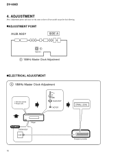
ADJUSTMENT Note: Adjustment points and items are the same as those of base model except for the following. 7ADJUSTMENT POINT AVJB ASSY SIDE A 1 VC131 1 18MHz Master Clock Adjustment 7ELECTRICAL ADJUSTMENT 1 18MHz Master Clock Adjustment • Normal mode • Power ON START DVDM ASSY Player IC813 6 16 AVJB ASSY VC131 27MHz ± 20Hz Frequency counter DV-606D 4.
ADJUSTMENT Note: Adjustment points and items are the same as those of base model except for the following. 7ADJUSTMENT POINT AVJB ASSY SIDE A 1 VC131 1 18MHz Master Clock Adjustment 7ELECTRICAL ADJUSTMENT 1 18MHz Master Clock Adjustment • Normal mode • Power ON START DVDM ASSY Player IC813 6 16 AVJB ASSY VC131 27MHz ± 20Hz Frequency counter DV-606D 4.
Service Manual
Page 17
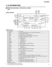
... *3 : Schmit Trigger input with Function Mode Controller Control I /O Function 1 LRCIN IN Left & right Clock Input. Analog Grand 15 VCC1 - Analog Power +5V 16 VOUTL OUT L-ch Analog Voltage Output of Oscillator. Digital Power +5V 9 VCC2R - Digital Grand 8 VDD - Equivalent to that shown in reset. *2 23 CS/IWO IN Chip Select/Input Format Selection. Analog Grand 11 EXTR OUT R-ch, Common Pin of Audio Signal 14 AGND1 - Non Connection 13 VOUTR OUT...
... *3 : Schmit Trigger input with Function Mode Controller Control I /O Function 1 LRCIN IN Left & right Clock Input. Analog Grand 15 VCC1 - Analog Power +5V 16 VOUTL OUT L-ch Analog Voltage Output of Oscillator. Digital Power +5V 9 VCC2R - Digital Grand 8 VDD - Equivalent to that shown in reset. *2 23 CS/IWO IN Chip Select/Input Format Selection. Analog Grand 11 EXTR OUT R-ch, Common Pin of Audio Signal 14 AGND1 - Non Connection 13 VOUTR OUT...