Design Guide
Page 17
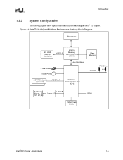
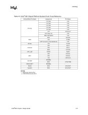
Intel® 820 Chipset Platform Performance Desktop Block Diagram Processor 4X AGP Graphics Controller AGP 2.0 82820 Memory Controller Hub (MCH) Main Memory 4 IDE Drives 2 USB Ports Hub Interface PCI Bus PCI Slots AC'97 Codec(s) (optional) AC'97 2.1 82801AA I/O Controller Hub (ICH) Keyboard, Mouse, FD, PP, SP, IR LPC I/F Super I/O FWH Flash BIOS GPIO Intel®820 Chipset Design Guide 1-5 Figure 1-1. Introduction 1.3.3 System Configuration The following figures show typical platform configurations using the Intel® 820 chipset.
Intel® 820 Chipset Platform Performance Desktop Block Diagram Processor 4X AGP Graphics Controller AGP 2.0 82820 Memory Controller Hub (MCH) Main Memory 4 IDE Drives 2 USB Ports Hub Interface PCI Bus PCI Slots AC'97 Codec(s) (optional) AC'97 2.1 82801AA I/O Controller Hub (ICH) Keyboard, Mouse, FD, PP, SP, IR LPC I/F Super I/O FWH Flash BIOS GPIO Intel®820 Chipset Design Guide 1-5 Figure 1-1. Introduction 1.3.3 System Configuration The following figures show typical platform configurations using the Intel® 820 chipset.
Design Guide
Page 34
... 28 Ω nominal impedance with a traditional 7 mil prepreg requires 28 mil wide traces. Refer to Section 5.3, "Stackup Requirement" on page 5-1 for the Intel® 820 chipset platform (refer to Section 5.3, "Stackup Requirement" on the Direct Rambus* Channel are : • RSL Signals - DQB[8:0] - CFM, CFM.... This thinner prepreg allows 18 mil wide traces to the termination. 2-8 Intel®820 Chipset Design Guide RQ[7:0] • CMOS Signals - CMD (high-speed CMOS signal) - All unpopulated slots must have continuity modules in place to ensure that the signals propagate to ...
... 28 Ω nominal impedance with a traditional 7 mil prepreg requires 28 mil wide traces. Refer to Section 5.3, "Stackup Requirement" on page 5-1 for the Intel® 820 chipset platform (refer to Section 5.3, "Stackup Requirement" on the Direct Rambus* Channel are : • RSL Signals - DQB[8:0] - CFM, CFM.... This thinner prepreg allows 18 mil wide traces to the termination. 2-8 Intel®820 Chipset Design Guide RQ[7:0] • CMOS Signals - CMD (high-speed CMOS signal) - All unpopulated slots must have continuity modules in place to ensure that the signals propagate to ...

Design Guide
Page 72
...board. Table 2-12 below provides segment descriptions and length recommendations for 133 MHz and 100 MHz 2-way processor/Intel® 820 chipset designs. An example topology is populated. For 2-way processor / Intel® 820 chipset designs, a termination card must be placed electrically in the unused slot... when only one processor is shown in Figure 2-36. Intel® Pentium® III Processor Dual Processor Configuration ...
...board. Table 2-12 below provides segment descriptions and length recommendations for 133 MHz and 100 MHz 2-way processor/Intel® 820 chipset designs. An example topology is populated. For 2-way processor / Intel® 820 chipset designs, a termination card must be placed electrically in the unused slot... when only one processor is shown in Figure 2-36. Intel® Pentium® III Processor Dual Processor Configuration ...
Design Guide
Page 81
... and decoupling are contained in "Slot 1 Processor Power Distribution Guidelines." • Special Case AGTL+ signals for simulation: There are contained in "Slot 1 Processor Power Distribution Guidelines." ...signals may violate the ringback specifications. When a signal is generated locally on the processor. Intel®820 Chipset Design Guide 2-55 Layout/Routing Guidelines Minimizing Crosstalk on the AGTL+ Interface...signals that have larger voltage swings, such as 5V PCI. • Select a board stack-up that can create a large undershoot, followed by more than the data lines...
... and decoupling are contained in "Slot 1 Processor Power Distribution Guidelines." • Special Case AGTL+ signals for simulation: There are contained in "Slot 1 Processor Power Distribution Guidelines." ...signals may violate the ringback specifications. When a signal is generated locally on the processor. Intel®820 Chipset Design Guide 2-55 Layout/Routing Guidelines Minimizing Crosstalk on the AGTL+ Interface...signals that have larger voltage swings, such as 5V PCI. • Select a board stack-up that can create a large undershoot, followed by more than the data lines...
Design Guide
Page 90
The motherboard can implement any SDATAIN signal that can be disabled via a hardware jumper or stuffing option, then its SDATAIN signal does not need a pull-down resistor to ground. • AMR Slot Special Connections - If however, the SDATAIN signal has no codec connected, or is connected to an AMR slot, or is connected to...
The motherboard can implement any SDATAIN signal that can be disabled via a hardware jumper or stuffing option, then its SDATAIN signal does not need a pull-down resistor to ground. • AMR Slot Special Connections - If however, the SDATAIN signal has no codec connected, or is connected to an AMR slot, or is connected to...
Design Guide
Page 129
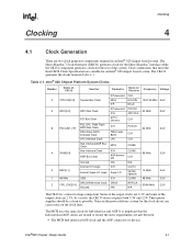
... 3.3V LPC Interface Clock LPC CLK Hub Interface/AGP Bus Clock MCH CLK66 4 3V66[0-3] Hub Interface Clock AGP Bus Clock Unused ICH AGP device/ slot N/A CLK66 CLK N/A 66 MHz 3.3V 2 REF[0-1] Internal ICH Logic ICH Internal Super I/O Logic Super I/O CLK14 Vendor Specific 14 MHz 3.3V ...ICH DRCG Reference Clock DRCG 2 CPU_DIV2[0-1] Unused N/A CLK48 REFCLK N/A 48 MHz 50/66 MHz 3.3V 2.5V The CK133 is important that meet the Intel CK98 Clock Specification are suitable for hub interface and AGP. Table 4-1. As a result, the CK133 device requires both 3.3V and 2.5V. It ...
... 3.3V LPC Interface Clock LPC CLK Hub Interface/AGP Bus Clock MCH CLK66 4 3V66[0-3] Hub Interface Clock AGP Bus Clock Unused ICH AGP device/ slot N/A CLK66 CLK N/A 66 MHz 3.3V 2 REF[0-1] Internal ICH Logic ICH Internal Super I/O Logic Super I/O CLK14 Vendor Specific 14 MHz 3.3V ...ICH DRCG Reference Clock DRCG 2 CPU_DIV2[0-1] Unused N/A CLK48 REFCLK N/A 48 MHz 50/66 MHz 3.3V 2.5V The CK133 is important that meet the Intel CK98 Clock Specification are suitable for hub interface and AGP. Table 4-1. As a result, the CK133 device requires both 3.3V and 2.5V. It ...
Design Guide
Page 130
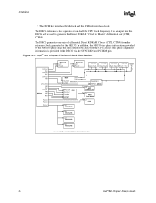
...of differential Direct RDRAM Clocks (CTM, CTM#) from the reference clock generated by the MCH to Master" differential pair (CTM, CTM#). Intel® 820 Chipset Platform Clock Distribution CPUCLK APIC CPUCLK APIC CPUCLK 3V66 CPU_DIV2 3V66 APIC PCICLK* 3V66 CK133 REF 48Hz PCICLK PCICLK PCICLK ... TERM RCLK TCLK MCH CTM CFM E F HCLKIN CLK66 PHASEINFO G APICCLK ICH H PCICLK I CLK66 J CLK14 K CLK48 L CLK PCI SLOTS L CLK PCI SLOTS L CLK PCI SLOTS L CLK PCI SLOTS PHASEINFO Q REFCLK DRCG P CLK AGP CONNECTOR N CLK FWH Flash BIOS M CLK LPC * The free-running PCI clock should be connected ...
...of differential Direct RDRAM Clocks (CTM, CTM#) from the reference clock generated by the MCH to Master" differential pair (CTM, CTM#). Intel® 820 Chipset Platform Clock Distribution CPUCLK APIC CPUCLK APIC CPUCLK 3V66 CPU_DIV2 3V66 APIC PCICLK* 3V66 CK133 REF 48Hz PCICLK PCICLK PCICLK ... TERM RCLK TCLK MCH CTM CFM E F HCLKIN CLK66 PHASEINFO G APICCLK ICH H PCICLK I CLK66 J CLK14 K CLK48 L CLK PCI SLOTS L CLK PCI SLOTS L CLK PCI SLOTS L CLK PCI SLOTS PHASEINFO Q REFCLK DRCG P CLK AGP CONNECTOR N CLK FWH Flash BIOS M CLK LPC * The free-running PCI clock should be connected ...
Design Guide
Page 132
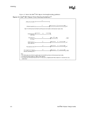
...connector to eliminate pin-to -pin skew. 3V66 Clock for Z AGP Slot PCI Clock for Z PCI Slots 3V66 Clock for Z MCH and ICH Z PCI Clock for ICH 1.5" 4" 4" ±TBD3 ±0" ±0" PCI Clock for On-Board Z Devices (excluding ICH) 4" ±TBD3 Note: 1. The TBD... 150ps/in trace velocity. 3. Intel® 820 Chipset Clock Routing Guidelines1,2 Y CPUCLK to SC242 Y CPUCLK to MCH 5.3" ±0" Note: Tie CPUCLK for a maximum of ±2ns clock skew. 820 lk t d 4-4 Intel®820 Chipset Design Guide Clocking Figure 4-2 shows the Intel® 820 chipset clock length ...
...connector to eliminate pin-to -pin skew. 3V66 Clock for Z AGP Slot PCI Clock for Z PCI Slots 3V66 Clock for Z MCH and ICH Z PCI Clock for ICH 1.5" 4" 4" ±TBD3 ±0" ±0" PCI Clock for On-Board Z Devices (excluding ICH) 4" ±TBD3 Note: 1. The TBD... 150ps/in trace velocity. 3. Intel® 820 Chipset Clock Routing Guidelines1,2 Y CPUCLK to SC242 Y CPUCLK to MCH 5.3" ±0" Note: Tie CPUCLK for a maximum of ±2ns clock skew. 820 lk t d 4-4 Intel®820 Chipset Design Guide Clocking Figure 4-2 shows the Intel® 820 chipset clock length ...
Design Guide
Page 133
...PCICLK-F CLK CLK GCLKIN CLK66 CLK CLK48 BCLK BCLK HCLKIN Refclk PICCLK PICCLK APICCLK CTM/CTM# HCLKOUT RCLKOUT Intel®820 Chipset Design Guide 4-5 Clocking Table 4-3. Intel® 820 Chipset Platform System Clock Cross-Reference CK133/DRCG Pin Name PCICLK 3V66 48 MHz CPUCLK CPU_div2 ...APIC Clk/ClkB1 CFM/CFM#1,2 PclkM SynclkN Component PCI Slot PCI Slot PCI Slot PCI Slot PCI Slot ICH LPC Super I/O FWH Flash BIOS MCH ICH AGP Connector (on-board device) ICH...
...PCICLK-F CLK CLK GCLKIN CLK66 CLK CLK48 BCLK BCLK HCLKIN Refclk PICCLK PICCLK APICCLK CTM/CTM# HCLKOUT RCLKOUT Intel®820 Chipset Design Guide 4-5 Clocking Table 4-3. Intel® 820 Chipset Platform System Clock Cross-Reference CK133/DRCG Pin Name PCICLK 3V66 48 MHz CPUCLK CPU_div2 ...APIC Clk/ClkB1 CFM/CFM#1,2 PclkM SynclkN Component PCI Slot PCI Slot PCI Slot PCI Slot PCI Slot ICH LPC Super I/O FWH Flash BIOS MCH ICH AGP Connector (on-board device) ICH...
Design Guide
Page 155
...-RAM) requires 7 power planes to be used . The requirements for each power plane are met using a switching regulator. On the Intel® 820 chipset Reference Board, the only devices connected to power the SC242 processor. VCCVID This power plane is used to the 5V Dual plane are so low... The maximum 2.5V tolerance is 125 mV, however during the maximum load-step of : • VRM 8.4 DC-DC Converter Design Guidelines • Slot 1 Power Delivery Guidelines Note: This regulator is derived from the 5V core ATX supply during Suspend-to-RAM and therefore, the VCMOS rail can be...
...-RAM) requires 7 power planes to be used . The requirements for each power plane are met using a switching regulator. On the Intel® 820 chipset Reference Board, the only devices connected to power the SC242 processor. VCCVID This power plane is used to the 5V Dual plane are so low... The maximum 2.5V tolerance is 125 mV, however during the maximum load-step of : • VRM 8.4 DC-DC Converter Design Guidelines • Slot 1 Power Delivery Guidelines Note: This regulator is derived from the 5V core ATX supply during Suspend-to-RAM and therefore, the VCMOS rail can be...
Design Guide
Page 157
...regulator is not required in a Intel® 820 chipset based system that during the initialization of the ICH and the PCI 3.3Vaux suspend power pins. All devices must be powered when the system is : • Full-power Operation: 375 mA * number of PCI slots • Suspend Operation: 375+...20 * (number of PCI slots - 1) In addition to the latest Intel® 820 Chipset: 82820 Memory Controller Hub (MCH) datasheet. 3.3VSB The 3.3VSB plane powers the ...
...regulator is not required in a Intel® 820 chipset based system that during the initialization of the ICH and the PCI 3.3Vaux suspend power pins. All devices must be powered when the system is : • Full-power Operation: 375 mA * number of PCI slots • Suspend Operation: 375+...20 * (number of PCI slots - 1) In addition to the latest Intel® 820 Chipset: 82820 Memory Controller Hub (MCH) datasheet. 3.3VSB The 3.3VSB plane powers the ...
Design Guide
Page 163
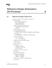
... RDRAM Memory Interface - 266 MHz, 300 MHz, 356 MHz and 400 MHz Direct RDRAM Support • 4 PCI Add-in Slots - Keyboard Controller • AC'97 Bus Connector and Audio Codec • WfM Support • Integrated System Management • ...Parallel Port, 2 Serial Ports - I /O - ACPI Rev. 1.0 Compliant - APM Rev. 1.2 Compliant • Pentium III on-board VRM 8.4 compliant regulator • 4 Layer Design Intel®820 Chipset Design Guide A-1 Reference Design Schematics: Uni-Processor Reference Design Schematics: Uni-Processor A A.1 Reference Design Feature Set The reference...
... RDRAM Memory Interface - 266 MHz, 300 MHz, 356 MHz and 400 MHz Direct RDRAM Support • 4 PCI Add-in Slots - Keyboard Controller • AC'97 Bus Connector and Audio Codec • WfM Support • Integrated System Management • ...Parallel Port, 2 Serial Ports - I /O - ACPI Rev. 1.0 Compliant - APM Rev. 1.2 Compliant • Pentium III on-board VRM 8.4 compliant regulator • 4 Layer Design Intel®820 Chipset Design Guide A-1 Reference Design Schematics: Uni-Processor Reference Design Schematics: Uni-Processor A A.1 Reference Design Feature Set The reference...
Design Guide
Page 183
... AD11 AD9 PCLK2 5 PREQ#1 8,32 AD31 AD29 AD27 AD25 C_BE#3 AD23 AD21 AD19 AD17 C_BE#2 IRDY# DEVSEL# PLOCK# PERR# SERR# C_BE#1 AD14 AD12 AD10 PCI Slot 1 J9 PCI3_CON B1 A1 B2 A2 B3 A3 B4 A4 B5 A5 B6 A6 B7 A7 B8 A8 B9 A9 B10 A10 B11 A11 B12... AD13 AD11 AD9 C_BE#0 AD6 AD4 AD16 R120 R_AD16 8,16 20 100 AD17 R119 R_AD17 8,16 20 100 AD2 AD0 A PU2_REQ64# 20 TITLE: INTEL(R) 820 CHIPSET CUSTOMER REFERENCE BOARD REV: PCI CONNECTORS 1 AND 2 1.01 R PCD PLATFORM DESIGN DRAWN BY: PROJECT: 1900 PRAIRIE CITY ROAD FOLSOM, CALIFORNIA 95630 LAST REVISED: SHEET: 11-18...
... AD11 AD9 PCLK2 5 PREQ#1 8,32 AD31 AD29 AD27 AD25 C_BE#3 AD23 AD21 AD19 AD17 C_BE#2 IRDY# DEVSEL# PLOCK# PERR# SERR# C_BE#1 AD14 AD12 AD10 PCI Slot 1 J9 PCI3_CON B1 A1 B2 A2 B3 A3 B4 A4 B5 A5 B6 A6 B7 A7 B8 A8 B9 A9 B10 A10 B11 A11 B12... AD13 AD11 AD9 C_BE#0 AD6 AD4 AD16 R120 R_AD16 8,16 20 100 AD17 R119 R_AD17 8,16 20 100 AD2 AD0 A PU2_REQ64# 20 TITLE: INTEL(R) 820 CHIPSET CUSTOMER REFERENCE BOARD REV: PCI CONNECTORS 1 AND 2 1.01 R PCD PLATFORM DESIGN DRAWN BY: PROJECT: 1900 PRAIRIE CITY ROAD FOLSOM, CALIFORNIA 95630 LAST REVISED: SHEET: 11-18...
Design Guide
Page 184
VCC5 PCI Slot 2 J12 PCI3_CON B1 A1 PTCK B2 A2 D 20,21 B3 A3 B4 A4 B5 A5 B6 A6 ...,16,19,20,21,22 PGNT#5 8,32 R110 REQ#A 8,32 0K No Stuff R110. 8 7 PCI Connectors 2 and 3 VCC3_3 VCC12- FCPGA REFERENCE BOARD REV: PCI CONNECTORS 3 AND 4 1.0 R PCD PLATFORM DESIGN DRAWN BY: PROJECT: 1900 PRAIRIE CITY ROAD FOLSOM, CALIFORNIA 95630 LAST REVISED: SHEET: 11...A58 AD0 B59 A59 A PU3_REQ64# 21 PU4_ACK64# 21 B60 A60 B61 A61 PU4_REQ64# 21 B62 A62 TITLE: INTEL(R) 820 CHIPSET - VCC5 PCI Slot 3 J11 PCI3_CON VCC5 VCC12 J9 must be furthest from the processor.
VCC5 PCI Slot 2 J12 PCI3_CON B1 A1 PTCK B2 A2 D 20,21 B3 A3 B4 A4 B5 A5 B6 A6 ...,16,19,20,21,22 PGNT#5 8,32 R110 REQ#A 8,32 0K No Stuff R110. 8 7 PCI Connectors 2 and 3 VCC3_3 VCC12- FCPGA REFERENCE BOARD REV: PCI CONNECTORS 3 AND 4 1.0 R PCD PLATFORM DESIGN DRAWN BY: PROJECT: 1900 PRAIRIE CITY ROAD FOLSOM, CALIFORNIA 95630 LAST REVISED: SHEET: 11...A58 AD0 B59 A59 A PU3_REQ64# 21 PU4_ACK64# 21 B60 A60 B61 A61 PU4_REQ64# 21 B62 A62 TITLE: INTEL(R) 820 CHIPSET - VCC5 PCI Slot 3 J11 PCI3_CON VCC5 VCC12 J9 must be furthest from the processor.
Design Guide
Page 198
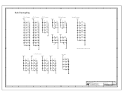
... 0.1UF 0.1UF 0.1UF 0.1UF 0.1UF Termination Decoupling VTT1_5 0.1UF 0.1UF 0.1UF 0.1UF 0.01UF 0.01UF 0.01UF 0.01UF Place caps at VTT pins on Slot 1 connector. 5 4 B A TITLE: INTEL(R) 820 CHIPSET CUSTOMER REFERENCE BOARD REV: BULK DECOUPLING 1.01 R PCD PLATFORM DESIGN DRAWN BY: PROJECT: 1900 PRAIRIE CITY ROAD FOLSOM, CALIFORNIA 95630 LAST REVISED: SHEET: 11-18...
... 0.1UF 0.1UF 0.1UF 0.1UF 0.1UF Termination Decoupling VTT1_5 0.1UF 0.1UF 0.1UF 0.1UF 0.01UF 0.01UF 0.01UF 0.01UF Place caps at VTT pins on Slot 1 connector. 5 4 B A TITLE: INTEL(R) 820 CHIPSET CUSTOMER REFERENCE BOARD REV: BULK DECOUPLING 1.01 R PCD PLATFORM DESIGN DRAWN BY: PROJECT: 1900 PRAIRIE CITY ROAD FOLSOM, CALIFORNIA 95630 LAST REVISED: SHEET: 11-18...
Design Guide
Page 203
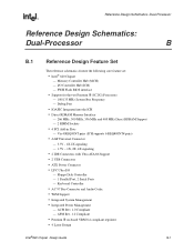
... • Integrated System Management • Integrated Power Management - APM Rev. 1.2 Compliant • Pentium III on-board VRM 8.4 compliant regulator • 4 Layer Design Intel®820 Chipset Design Guide B-1 Debug Port • IOAPIC Integrated into the ICH • Direct RDRAM Memory Interface... - 266 MHz, 300 MHz, 356 MHz and 400 MHz Direct RDRAM Support - 2 RIMM Sockets • 4 PCI Add-in Slots - Memory Controller Hub...
... • Integrated System Management • Integrated Power Management - APM Rev. 1.2 Compliant • Pentium III on-board VRM 8.4 compliant regulator • 4 Layer Design Intel®820 Chipset Design Guide B-1 Debug Port • IOAPIC Integrated into the ICH • Direct RDRAM Memory Interface... - 266 MHz, 300 MHz, 356 MHz and 400 MHz Direct RDRAM Support - 2 RIMM Sockets • 4 PCI Add-in Slots - Memory Controller Hub...

Design Guide
Page 225
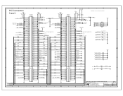
VCC5 PCI Slot 0 J12 PCI3_CON B1 A1 PTCK B2 A2 D 22,23 B3 A3 B4 A4 B5 A5 B6 A6 10... AD31 AD29 AD27 AD25 C_BE#3 AD23 AD21 AD19 AD17 C_BE#2 IRDY# DEVSEL# PLOCK# PERR# SERR# C_BE#1 AD14 AD12 AD10 PCI Slot 1 J11 PCI3_CON B1 A1 B2 A2 B3 A3 B4 A4 B5 A5 B6 A6 B7 A7 B8 A8 B9 A9 B10 A10 B11 ... 10,18,22,23 22 100 AD17 R119 R_AD17 10,18,22,23 22 100 AD2 AD0 A PU2_REQ64# 22 TITLE: INTEL(R) 820 CHIPSET DUAL PROCESSOR CUSTOMER REFERENCE BOARD REV: PCI CONNECTORS 1 AND 2 3.03 R PCD PLATFORM DESIGN DRAWN BY: PROJECT: 1900 PRAIRIE CITY ROAD FOLSOM, CALIFORNIA...
VCC5 PCI Slot 0 J12 PCI3_CON B1 A1 PTCK B2 A2 D 22,23 B3 A3 B4 A4 B5 A5 B6 A6 10... AD31 AD29 AD27 AD25 C_BE#3 AD23 AD21 AD19 AD17 C_BE#2 IRDY# DEVSEL# PLOCK# PERR# SERR# C_BE#1 AD14 AD12 AD10 PCI Slot 1 J11 PCI3_CON B1 A1 B2 A2 B3 A3 B4 A4 B5 A5 B6 A6 B7 A7 B8 A8 B9 A9 B10 A10 B11 ... 10,18,22,23 22 100 AD17 R119 R_AD17 10,18,22,23 22 100 AD2 AD0 A PU2_REQ64# 22 TITLE: INTEL(R) 820 CHIPSET DUAL PROCESSOR CUSTOMER REFERENCE BOARD REV: PCI CONNECTORS 1 AND 2 3.03 R PCD PLATFORM DESIGN DRAWN BY: PROJECT: 1900 PRAIRIE CITY ROAD FOLSOM, CALIFORNIA...

Design Guide
Page 226
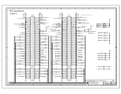
... B62 A62 10,18,22 C_BE#[3:0] 10,18,22 AD[31:0] 8 7 key key 6 5 4 3 2 1 VCC3_3 VCC3_3 VCC3_3 VCC5 VCC12 VCC12- VCC5 PCI Slot 3 J9 PCI3_CON VCC5 VCC12 J9 must be furthest from the processor. PTRST# 22,23 PTMS PTDI 22,23 22,23 22,23 PTCK B1 A1...A57 AD2 AD0 AD1 B58 A58 AD0 B59 A59 A PU3_REQ64# 23 PU4_ACK64# 23 B60 A60 B61 A61 PU4_REQ64# 23 B62 A62 TITLE: INTEL(R) 820 CHIPSET DUAL PROCESSOR CUSTOMER REFERENCE BOARD REV: PCI CONNECTORS 3 AND 4 3.03 R PCD PLATFORM DESIGN DRAWN BY: PROJECT: 1900 PRAIRIE CITY ROAD FOLSOM, CALIFORNIA 95630 LAST REVISED...
... B62 A62 10,18,22 C_BE#[3:0] 10,18,22 AD[31:0] 8 7 key key 6 5 4 3 2 1 VCC3_3 VCC3_3 VCC3_3 VCC5 VCC12 VCC12- VCC5 PCI Slot 3 J9 PCI3_CON VCC5 VCC12 J9 must be furthest from the processor. PTRST# 22,23 PTMS PTDI 22,23 22,23 22,23 PTCK B1 A1...A57 AD2 AD0 AD1 B58 A58 AD0 B59 A59 A PU3_REQ64# 23 PU4_ACK64# 23 B60 A60 B61 A61 PU4_REQ64# 23 B62 A62 TITLE: INTEL(R) 820 CHIPSET DUAL PROCESSOR CUSTOMER REFERENCE BOARD REV: PCI CONNECTORS 3 AND 4 3.03 R PCD PLATFORM DESIGN DRAWN BY: PROJECT: 1900 PRAIRIE CITY ROAD FOLSOM, CALIFORNIA 95630 LAST REVISED...
Design Guide
Page 240
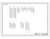
...0.1UF 0.1UF 0.1UF 0.1UF 0.01UF 0.1UF 0.1UF 0.1UF 0.1UF C371 1 2 + 22UF C367 2 1 + 22UF Place caps at VTT pins on Slot 1 connector. VCCVID Core Voltage Decoupling VCCVID VCCVID1 VCCVID1 VCC3_3SBY B 0.1UF 10UF 10UF 10UF 10UF 10UF 10UF 10UF 10UF 0.1UF 10UF 10UF 10UF 10UF 0.1UF 10UF...C114 C64 C345 C344 C343 C342 C364 C363 C357 C351 C346 C365 C149 C150 C151 C152 C153 A A TITLE: INTEL(R) 820 CHIPSET DUAL PROCESSOR CUSTOMER REFERENCE BOARD REV: BULK DECOUPLING 3.03 R PCD PLATFORM DESIGN DRAWN BY: PROJECT: 1900 PRAIRIE CITY ROAD FOLSOM, CALIFORNIA 95630...
...0.1UF 0.1UF 0.1UF 0.1UF 0.01UF 0.1UF 0.1UF 0.1UF 0.1UF C371 1 2 + 22UF C367 2 1 + 22UF Place caps at VTT pins on Slot 1 connector. VCCVID Core Voltage Decoupling VCCVID VCCVID1 VCCVID1 VCC3_3SBY B 0.1UF 10UF 10UF 10UF 10UF 10UF 10UF 10UF 10UF 0.1UF 10UF 10UF 10UF 10UF 0.1UF 10UF...C114 C64 C345 C344 C343 C342 C364 C363 C357 C351 C346 C365 C149 C150 C151 C152 C153 A A TITLE: INTEL(R) 820 CHIPSET DUAL PROCESSOR CUSTOMER REFERENCE BOARD REV: BULK DECOUPLING 3.03 R PCD PLATFORM DESIGN DRAWN BY: PROJECT: 1900 PRAIRIE CITY ROAD FOLSOM, CALIFORNIA 95630...

