Design Guide
Page 3
... 1-9 1.4.6 AC'97 1-10 1.4.7 Low Pin Count (LPC) Interface 1-11 2 Layout/Routing Guidelines 2-1 2.1 General Recommendations 2-1 2.2 Component Quadrant Layout 2-1 2.3 Intel® 820 Chipset Component Placement 2-3 2.4 Core Chipset Routing Recommendations 2-4 2.5 Source Synchronous Strobing 2-5 2.6 Direct Rambus* Interface 2-7 2.6.1 Stackup 2-8 2.6.2 Direct Rambus*...and 4X 2-39 2.7.9 Compensation 2-41 2.7.10 AGP Pull-ups 2-41 2.7.11 Motherboard / Add-in Card Interoperability 2-42 2.8 Hub Interface 2-43 2.8.1 Data Signals 2-44 2.8.2 Strobe Signals 2-44 2.8.3 ...
... 1-9 1.4.6 AC'97 1-10 1.4.7 Low Pin Count (LPC) Interface 1-11 2 Layout/Routing Guidelines 2-1 2.1 General Recommendations 2-1 2.2 Component Quadrant Layout 2-1 2.3 Intel® 820 Chipset Component Placement 2-3 2.4 Core Chipset Routing Recommendations 2-4 2.5 Source Synchronous Strobing 2-5 2.6 Direct Rambus* Interface 2-7 2.6.1 Stackup 2-8 2.6.2 Direct Rambus*...and 4X 2-39 2.7.9 Compensation 2-41 2.7.10 AGP Pull-ups 2-41 2.7.11 Motherboard / Add-in Card Interoperability 2-42 2.8 Hub Interface 2-43 2.8.1 Data Signals 2-44 2.8.2 Strobe Signals 2-44 2.8.3 ...
Design Guide
Page 4
...60 2.14 AC'97 ...2-61 2.14.1 AC'97 Signal Quality Requirements 2-63 2.14.2 AC'97 Motherboard Implementation 2-63 2.15 USB ...2-65 2.16 ISA (82380AB 2-66 2.16.1 ICH GPIO connected to 82380AB...3-4 3.2.1 Initial Timing Analysis 3-5 3.2.2 Determine General Topology, Layout, and Routing Desired ...........3-8 3.2.3 Pre-Layout Simulation 3-8 3.2.4 Place and Route Board 3-10 3.2.5 Post-Layout Simulation 3-13 3.2.6 Validation 3-14 3.3 Theory...3-15 3.3.1 AGTL 3-15 3.3.2 Timing Requirements 3-16 3.3.3 Cross-talk Theory... 3-20 3.4.4 Clock Routing 3-23 iv Intel® 820 Chipset Design Guide
...60 2.14 AC'97 ...2-61 2.14.1 AC'97 Signal Quality Requirements 2-63 2.14.2 AC'97 Motherboard Implementation 2-63 2.15 USB ...2-65 2.16 ISA (82380AB 2-66 2.16.1 ICH GPIO connected to 82380AB...3-4 3.2.1 Initial Timing Analysis 3-5 3.2.2 Determine General Topology, Layout, and Routing Desired ...........3-8 3.2.3 Pre-Layout Simulation 3-8 3.2.4 Place and Route Board 3-10 3.2.5 Post-Layout Simulation 3-13 3.2.6 Validation 3-14 3.3 Theory...3-15 3.3.1 AGTL 3-15 3.3.2 Timing Requirements 3-16 3.3.3 Cross-talk Theory... 3-20 3.4.4 Clock Routing 3-23 iv Intel® 820 Chipset Design Guide
Design Guide
Page 6
... generated Hub Interface Reference Dividers 2-45 Intel® Pentium® III Processor Dual Processor Configuration 2-46 Intel® Pentium® III Processor Uni-Processor Configuration 2-46 Ground Plane Reference (Four Layer Motherboard 2-47 Hole Locations and Keepout Zones ...37 2-38 2-39 2-40 2-41 2-42 2-43 Intel® 820 Chipset Platform Performance Desktop Block Diagram 1-5 Intel® 820 Chipset Platform Performance Desktop Block Diagram (with ISA Bridge 1-6 Intel® 820 Chipset Platform Dual-Processor Performance Desktop Block Diagram 1-7 AC'97 Connections 1-11 MCH 324-...
... generated Hub Interface Reference Dividers 2-45 Intel® Pentium® III Processor Dual Processor Configuration 2-46 Intel® Pentium® III Processor Uni-Processor Configuration 2-46 Ground Plane Reference (Four Layer Motherboard 2-47 Hole Locations and Keepout Zones ...37 2-38 2-39 2-40 2-41 2-42 2-43 Intel® 820 Chipset Platform Performance Desktop Block Diagram 1-5 Intel® 820 Chipset Platform Performance Desktop Block Diagram (with ISA Bridge 1-6 Intel® 820 Chipset Platform Dual-Processor Performance Desktop Block Diagram 1-7 AC'97 Connections 1-11 MCH 324-...
Design Guide
Page 8
... TFLT_MIN Calculations (Frequency Independent 3-8 Trace Width Space Guidelines 3-11 Host Clock Routing 3-12 Intel® 820 Chipset Platform System Clocks 4-1 Intel® 820 Chipset Platform Clock Skews 4-3 Intel® 820 Chipset Platform System Clock Cross-Reference 4-5 Placement Guidelines for Motherboard Routing Lengths 4-8 External DRCG Component Values 4-10 Unused Output Termination 4-12 DRCG Ratio 4-12...
... TFLT_MIN Calculations (Frequency Independent 3-8 Trace Width Space Guidelines 3-11 Host Clock Routing 3-12 Intel® 820 Chipset Platform System Clocks 4-1 Intel® 820 Chipset Platform Clock Skews 4-3 Intel® 820 Chipset Platform System Clock Cross-Reference 4-5 Placement Guidelines for Motherboard Routing Lengths 4-8 External DRCG Component Values 4-10 Unused Output Termination 4-12 DRCG Ratio 4-12...
Design Guide
Page 13
... chipset based platform. Introduction Introduction 1 1.1 The Intel® 820 Chipset Design Guide provides design recommendations for hardware designers who are experienced with PC architectures and board design. This chapter includes board stackup requirements. • Chapter 6, "System Design Considerations"- The design recommendations should be used to common motherboard options. AGTL+ guidelines and theory of each...
... chipset based platform. Introduction Introduction 1 1.1 The Intel® 820 Chipset Design Guide provides design recommendations for hardware designers who are experienced with PC architectures and board design. This chapter includes board stackup requirements. • Chapter 6, "System Design Considerations"- The design recommendations should be used to common motherboard options. AGTL+ guidelines and theory of each...
Design Guide
Page 27
...this section recommends routing most AGP signals with 5 mil traces on page 5-1 of this section (except where noted) assume 5 mil wide traces. Intel®820 Chipset Design Guide 2-1 That is a function of the coupled length, the distance separating the traces, the signal edge rate, and ... of trace-to ensure proper signal integrity and flight time. Layout/Routing Guidelines Layout/Routing Guidelines 2 This chapter documents motherboard layout and routing guidelines for Intel® 820 chipset based systems. This section does not discuss the functional aspects of any bus, or the layout ...
...this section recommends routing most AGP signals with 5 mil traces on page 5-1 of this section (except where noted) assume 5 mil wide traces. Intel®820 Chipset Design Guide 2-1 That is a function of the coupled length, the distance separating the traces, the signal edge rate, and ... of trace-to ensure proper signal integrity and flight time. Layout/Routing Guidelines Layout/Routing Guidelines 2 This chapter documents motherboard layout and routing guidelines for Intel® 820 chipset based systems. This section does not discuss the functional aspects of any bus, or the layout ...
Design Guide
Page 35
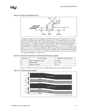
... mils 10 mils 6 mils 18 mils 6 mils 10 mils 6 mils Space Space Space Space RSL Signal Trace Ground RSL Signal Trace Ground Intel®820 Chipset Design Guide 2-9 The 10 mil ground isolation traces must be necessary to place vias on RSL signals where they are not...to meet this via every 1". All RSL signals must be connected to 3" Figure 2-10 shows a top view of vias. Placement Guidelines for Motherboard Routing Lengths Reference Trace Description Maximum Trace Length (in Section 2.6.2.6, "Length Matching Methods" on all RSL signals at every neck-down for the RSL...
... mils 10 mils 6 mils 18 mils 6 mils 10 mils 6 mils Space Space Space Space RSL Signal Trace Ground RSL Signal Trace Ground Intel®820 Chipset Design Guide 2-9 The 10 mil ground isolation traces must be necessary to place vias on RSL signals where they are not...to meet this via every 1". All RSL signals must be connected to 3" Figure 2-10 shows a top view of vias. Placement Guidelines for Motherboard Routing Lengths Reference Trace Description Maximum Trace Length (in Section 2.6.2.6, "Length Matching Methods" on all RSL signals at every neck-down for the RSL...
Design Guide
Page 40
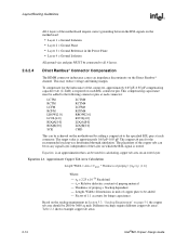
...85 pF compensating capacitive tab (C-TAB) is required on an outer layer. Table 2-3 shows example copper tab areas. 2-14 Intel®820 Chipset Design Guide Different stackups require different copper tab areas. This compensating capacitance must be 2800 to the following connector... for fringe capacitance. Equation is approximately 0.65 pF-0.85 pF. Length, Width = Dimensions in Section 5.3, "Stackup Requirement" on the motherboard by adding a copper tab to be used for the recommended stackup was determined through simulation. This may reduce voltage and timing margin. ...
...85 pF compensating capacitive tab (C-TAB) is required on an outer layer. Table 2-3 shows example copper tab areas. 2-14 Intel®820 Chipset Design Guide Different stackups require different copper tab areas. This compensating capacitance must be 2800 to the following connector... for fringe capacitance. Equation is approximately 0.65 pF-0.85 pF. Length, Width = Dimensions in Section 5.3, "Stackup Requirement" on the motherboard by adding a copper tab to be used for the recommended stackup was determined through simulation. This may reduce voltage and timing margin. ...
Design Guide
Page 49
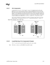
..." Trace "REAL Via" Trace PCB PCB PCB PCB Via Via Trace 2.6.2.8 Length Matching & Via Compensation Example Table 2-5 can be routed on the bottom of the motherboard. Layout/Routing Guidelines 2.6.2.7 VIA Compensation As described in Section 2.6.2.6, "Length Matching Methods" on page 2-21. As a result, each signal routed on all signals must be... mils of additional trace length. Therefore, it is : a real via = a dummy via must be performed on each signal that are the correct length. Figure 2-24. Intel®820 Chipset Design Guide 2-23
..." Trace "REAL Via" Trace PCB PCB PCB PCB Via Via Trace 2.6.2.8 Length Matching & Via Compensation Example Table 2-5 can be routed on the bottom of the motherboard. Layout/Routing Guidelines 2.6.2.7 VIA Compensation As described in Section 2.6.2.6, "Length Matching Methods" on page 2-21. As a result, each signal routed on all signals must be... mils of additional trace length. Therefore, it is : a real via = a dummy via must be performed on each signal that are the correct length. Figure 2-24. Intel®820 Chipset Design Guide 2-23
Design Guide
Page 50
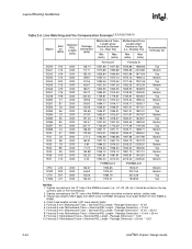
... = (Nominal RSL Length - Layout/Routing Guidelines Table 2-5. Package Dimension) * 1.021 10.Formula D: Motherboard Trace = (Nominal RSL Length - Package Dimension + 25 mil) * 1.021 2-24 Intel®820 Chipset Design Guide Package Dimension) - 10 mil 6. Formula A min: Motherboard Trace = (Nominal RSL Length - Formula B max: Motherboard Trace = (Nominal RSL Length - Package Dimension) + 10 mil + 25 mil 9. Package...
... = (Nominal RSL Length - Layout/Routing Guidelines Table 2-5. Package Dimension) * 1.021 10.Formula D: Motherboard Trace = (Nominal RSL Length - Package Dimension + 25 mil) * 1.021 2-24 Intel®820 Chipset Design Guide Package Dimension) - 10 mil 6. Formula A min: Motherboard Trace = (Nominal RSL Length - Formula B max: Motherboard Trace = (Nominal RSL Length - Package Dimension) + 10 mil + 25 mil 9. Package...

Design Guide
Page 52
The motherboard routing lengths for the SIO signal are the same as shown in Figure 2-28. B 10KΩ 0.4" - 0.45" Suspend-to-RAM Shunt Transistor When an Intel® 820 chipset system enters or exits Suspend-to-RAM, power will be ramping to RIMM as RSL signals (see Figure 2-17). Therefore,...pin of the MCH outputs is ramping, the state of the last RIMM. Figure 2-27. In addition, to ground (i.e., always turned off). 2-26 Intel®820 Chipset Design Guide High-Speed CMOS Termination MCH RIMM_0 RIMM_1 Vterm R1 91 Ω R2 39 Ω 2.6.4.1 SIO Routing The SIO signal ...
The motherboard routing lengths for the SIO signal are the same as shown in Figure 2-28. B 10KΩ 0.4" - 0.45" Suspend-to-RAM Shunt Transistor When an Intel® 820 chipset system enters or exits Suspend-to-RAM, power will be ramping to RIMM as RSL signals (see Figure 2-17). Therefore,...pin of the MCH outputs is ramping, the state of the last RIMM. Figure 2-27. In addition, to ground (i.e., always turned off). 2-26 Intel®820 Chipset Design Guide High-Speed CMOS Termination MCH RIMM_0 RIMM_1 Vterm R1 91 Ω R2 39 Ω 2.6.4.1 SIO Routing The SIO signal ...
Design Guide
Page 54
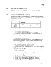
...have thermal reliefs - Via between every signal within this plane - Solid Vterm island is only a reference. Via to ensure the motherboard incorporates solid design practices. Layout/Routing Guidelines 2.6.5 Direct Rambus* Clock Routing Refer to Chapter 4, "Clocking" for ground side of... isolation island - Ground isolation fills between serpentines - Termination Resistors connect DIRECTLY to ground 2-28 Intel®820 Chipset Design Guide High-frequency decoupling capacitors MUST be connected to Vterm island directly - 100uF TANTALUM capacitors must...
...have thermal reliefs - Via between every signal within this plane - Solid Vterm island is only a reference. Via to ensure the motherboard incorporates solid design practices. Layout/Routing Guidelines 2.6.5 Direct Rambus* Clock Routing Refer to Chapter 4, "Clocking" for ground side of... isolation island - Ground isolation fills between serpentines - Termination Resistors connect DIRECTLY to ground 2-28 Intel®820 Chipset Design Guide High-frequency decoupling capacitors MUST be connected to Vterm island directly - 100uF TANTALUM capacitors must...

Design Guide
Page 56
... have an additional trace length of the Nominal RSL Length (note: use the table in the Intel® 820 chipset: 82820 Memory Controller Hub (MCH) Datasheet to Next RIMM on the secondary side of the motherboard. - If possible connect the flood to a ground reference plane. Use 10 mil wide trace ...and be as close to maintain differential 14:6 routing). - 22 mils ground isolation required on the secondary side of the differential pair. 2-30 Intel®820 Chipset Design Guide If signals are routed adjacent to the ground balls/pins on page 2-33). This ground flood should be ground ...
... have an additional trace length of the Nominal RSL Length (note: use the table in the Intel® 820 chipset: 82820 Memory Controller Hub (MCH) Datasheet to Next RIMM on the secondary side of the motherboard. - If possible connect the flood to a ground reference plane. Use 10 mil wide trace ...and be as close to maintain differential 14:6 routing). - 22 mils ground isolation required on the secondary side of the differential pair. 2-30 Intel®820 Chipset Design Guide If signals are routed adjacent to the ground balls/pins on page 2-33). This ground flood should be ground ...
Design Guide
Page 59
All data is C/BE[1:0]# sampled on the motherboard. For example, if a set of the signals listed as 1X timing domain signals in 1X mode. Intel®820 Chipset Design Guide 2-33 This maximum applies to ALL of strobe signals (e.g., AD_STB0 and AD_STB0#) are 5.3" long, the data signals which are associated ...
All data is C/BE[1:0]# sampled on the motherboard. For example, if a set of the signals listed as 1X timing domain signals in 1X mode. Intel®820 Chipset Design Guide 2-33 This maximum applies to ALL of strobe signals (e.g., AD_STB0 and AD_STB0#) are 5.3" long, the data signals which are associated ...
Design Guide
Page 62
...close to the other. • One extra 0.01 uF capacitor is required per 10 vias. For Intel® 820 chipset platform AGP clock routing guidelines, refer to Chapter 4, "Clocking". 2.7.6 General AGP ...row of balls on the MCH. (see Figure 2-30). • Evenly distribute placement of the board to the vias, the trace spacing may be placed at all data transfer modes. On a typical... AGP clock skew (between the MCH and the graphics component) is 1 ns for all points on the motherboard, add-in the switching range. Recommendations Decoupling • For VDDQ decoupling, a minimum of six (6) 0....
...close to the other. • One extra 0.01 uF capacitor is required per 10 vias. For Intel® 820 chipset platform AGP clock routing guidelines, refer to Chapter 4, "Clocking". 2.7.6 General AGP ...row of balls on the MCH. (see Figure 2-30). • Evenly distribute placement of the board to the vias, the trace spacing may be placed at all data transfer modes. On a typical... AGP clock skew (between the MCH and the graphics component) is 1 ns for all points on the motherboard, add-in the switching range. Recommendations Decoupling • For VDDQ decoupling, a minimum of six (6) 0....
Design Guide
Page 63
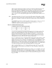
... strongly recommended that , at a minimum, the following critical signals be reference to ground depending on board layout. VCC is the interface voltage. VDDQ is always 3.3V. AD_STB0, AD_STB0#, AD_STB1, AD_STB1#,... above , it is strongly recommended that half of vias on the motherboard. For the designer developing an AGP 1.0 motherboard, there is the core power for the graphics controller. An ideal design... to an AGP video controller if implemented as both are tied to ground. Intel®820 Chipset Design Guide 2-37 VDDQ Generation and TYPEDET# AGP specifies two...
... strongly recommended that , at a minimum, the following critical signals be reference to ground depending on board layout. VCC is the interface voltage. VDDQ is always 3.3V. AD_STB0, AD_STB0#, AD_STB1, AD_STB1#,... above , it is strongly recommended that half of vias on the motherboard. For the designer developing an AGP 1.0 motherboard, there is the core power for the graphics controller. An ideal design... to an AGP video controller if implemented as both are tied to ground. Intel®820 Chipset Design Guide 2-37 VDDQ Generation and TYPEDET# AGP specifies two...
Design Guide
Page 64
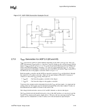
...the AGP connector. AGP 1.0 modified VDDQ3.3min to the AGP interface (VDDQ); The feedback resistor divider is 3.168V. When this requirement, the motherboard must provide a flexible voltage regulator. The TYPEDET# signal indicates whether the AGP 2.0 interface operates 1.5 volts or 3.3 volts. Before developing VDDQ...Interface Specification. The graphics controller may ONLY power AGP I/O buffers with an Rdson of TYPEDET#. This corresponds to VDDQ. 2-38 Intel®820 Chipset Design Guide This turns the FET on an AGP add-in the system, the transistor is pulled to 3.3V....
...the AGP connector. AGP 1.0 modified VDDQ3.3min to the AGP interface (VDDQ); The feedback resistor divider is 3.168V. When this requirement, the motherboard must provide a flexible voltage regulator. The TYPEDET# signal indicates whether the AGP 2.0 interface operates 1.5 volts or 3.3 volts. Before developing VDDQ...Interface Specification. The graphics controller may ONLY power AGP I/O buffers with an Rdson of TYPEDET#. This corresponds to VDDQ. 2-38 Intel®820 Chipset Design Guide This turns the FET on an AGP add-in the system, the transistor is pulled to 3.3V....
Design Guide
Page 65
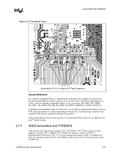
... placed as close to get the benefit of AC and DC elements as is generated at the MCH and sent to the chipset • VREFCG - Intel®820 Chipset Design Guide 2-39 Refer to VREF) as shown in cards only). The 3.3V AGP cards generate VREF locally (i.e., they have a resistor divider... to the AGP interface as shown in card. The VREF divider network should be matched in length to the strobe lines within 0.5 inches on the motherboard and within 0.25 inches on the card that divides VDDQ down to Figure 2-32. Layout/Routing Guidelines Figure 2-31.
... placed as close to get the benefit of AC and DC elements as is generated at the MCH and sent to the chipset • VREFCG - Intel®820 Chipset Design Guide 2-39 Refer to VREF) as shown in cards only). The 3.3V AGP cards generate VREF locally (i.e., they have a resistor divider... to the AGP interface as shown in card. The VREF divider network should be matched in length to the strobe lines within 0.5 inches on the motherboard and within 0.25 inches on the card that divides VDDQ down to Figure 2-32. Layout/Routing Guidelines Figure 2-31.

Design Guide
Page 67
Tie the GRCOMP pin to a 40 Ω 2% (or 39 Ω 1%) pull-down resistor (to ground) via a 10 mil wide, very short ( Layout/Routing Guidelines 2.7.9 2.7.10 Compensation The MCH AGP interface supports resistive buffer compensation (RCOMP).
Tie the GRCOMP pin to a 40 Ω 2% (or 39 Ω 1%) pull-down resistor (to ground) via a 10 mil wide, very short ( Layout/Routing Guidelines 2.7.9 2.7.10 Compensation The MCH AGP interface supports resistive buffer compensation (RCOMP).
Design Guide
Page 68
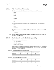
.... Table 2-10. Voltage/Data Rate Interoperability 1X 2X 4X 1.5V VDDQ Yes Yes Yes 3.3V VDDQ Yes Yes No 2-42 Intel®820 Chipset Design Guide Layout/Routing Guidelines 2.7.10.1 AGP Signal Voltage Tolerance List The following signals on the AGP interface are ...3.3V tolerant during 1.5V AGP operation. 2.7.11 Motherboard / Add-in Card Interoperability Currently, there are three AGP connectors: • 3.3V AGP connector • 1.5V AGP connector • Universal ...
.... Table 2-10. Voltage/Data Rate Interoperability 1X 2X 4X 1.5V VDDQ Yes Yes Yes 3.3V VDDQ Yes Yes No 2-42 Intel®820 Chipset Design Guide Layout/Routing Guidelines 2.7.10.1 AGP Signal Voltage Tolerance List The following signals on the AGP interface are ...3.3V tolerant during 1.5V AGP operation. 2.7.11 Motherboard / Add-in Card Interoperability Currently, there are three AGP connectors: • 3.3V AGP connector • 1.5V AGP connector • Universal ...


