
Service Manual
Page 28
... ▶ LSU Interface Module for Interfacing PVC with LSU ▶ 2 Channel General Purpose DMA Controller for High Speed I/O ▶ Dual Memory Bus Architecture - POWER ON RESET TIME : 6.6ms below (b) Memory 1) Flash Memory Store System Program and can be download System Program through PC Interface - Capacity : 0.5M Byte - Product spec and feature..., use Band Buffer, System Working Memory Area . - 8M capa : 8M Byte basic 8M :Printing System Working Memory Area Access Time : 60 nsec Service Manual 2-18 Samsung Electronics
... ▶ LSU Interface Module for Interfacing PVC with LSU ▶ 2 Channel General Purpose DMA Controller for High Speed I/O ▶ Dual Memory Bus Architecture - POWER ON RESET TIME : 6.6ms below (b) Memory 1) Flash Memory Store System Program and can be download System Program through PC Interface - Capacity : 0.5M Byte - Product spec and feature..., use Band Buffer, System Working Memory Area . - 8M capa : 8M Byte basic 8M :Printing System Working Memory Area Access Time : 60 nsec Service Manual 2-18 Samsung Electronics

Service Manual
Page 108
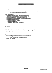
System Diagram 5.1 Block Diagram 5-1 Samsung Electronics Service Manual Soft POWER Tact Switch CANCEL Tact Switch Error Ready JAM 24V TOP Cover Micro Switch 24VS +3.3V / +24V AC INLET FUSER CONTROL ... FUSER Unit 16P LSU CONTROL SDRAM (8MByte) EEPROM (4Kbit) Stepper Motor Controller IC MAIN Controller Jupiter4E Core : 150MHz ARM940T-32bit RISC Clock Generator CLK 12MHz RESET IC USB Device THERMISTOR 2P 4P 2P MT STEP Main Motor SOL PickUp Clutch 5P FEED Sensor EMPTY Sensor System Diagram 5.
System Diagram 5.1 Block Diagram 5-1 Samsung Electronics Service Manual Soft POWER Tact Switch CANCEL Tact Switch Error Ready JAM 24V TOP Cover Micro Switch 24VS +3.3V / +24V AC INLET FUSER CONTROL ... FUSER Unit 16P LSU CONTROL SDRAM (8MByte) EEPROM (4Kbit) Stepper Motor Controller IC MAIN Controller Jupiter4E Core : 150MHz ARM940T-32bit RISC Clock Generator CLK 12MHz RESET IC USB Device THERMISTOR 2P 4P 2P MT STEP Main Motor SOL PickUp Clutch 5P FEED Sensor EMPTY Sensor System Diagram 5.


