

Service Manual
Page 24
...RF_WCDMA_PWRDET_EN Y10 ADC_I_NEG W10 ADC_I_POS W9 ADC_Q_NEG Y9 ADC_Q_POS Y8 DAC_I_NEG W8 DAC_I_POS W7 DAC_Q_NEG Y7 DAC_Q_POS AB7 TX_POW Copyright © 2007 LG Electronics. LGE Internal Use Only Asta Interface Asta controls GSM RF part using these signals through GSM RF chip-Gimli. •...Figure 3-1- 5. Only for connecting a Camera module. XGAM Subsystem The XGAM subsystem is responsible for clock generation and clock and reset distribution within the digital baseband controller. Schematic of this data to external devices. Technical Brief E. The visual data could be...
...RF_WCDMA_PWRDET_EN Y10 ADC_I_NEG W10 ADC_I_POS W9 ADC_Q_NEG Y9 ADC_Q_POS Y8 DAC_I_NEG W8 DAC_I_POS W7 DAC_Q_NEG Y7 DAC_Q_POS AB7 TX_POW Copyright © 2007 LG Electronics. LGE Internal Use Only Asta Interface Asta controls GSM RF part using these signals through GSM RF chip-Gimli. •...Figure 3-1- 5. Only for connecting a Camera module. XGAM Subsystem The XGAM subsystem is responsible for clock generation and clock and reset distribution within the digital baseband controller. Schematic of this data to external devices. Technical Brief E. The visual data could be...
Service Manual
Page 25
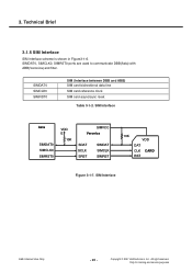
... Use Only - 26 - SIMDAT0 SIMCLK0 SIMRST0 SIM (Interface between DBB and ABB) SIM card bidirectional data line SIM card reference clock SIM card async/sync reset Table 3-1-2. All right reserved. Copyright © 2007...
... Use Only - 26 - SIMDAT0 SIMCLK0 SIMRST0 SIM (Interface between DBB and ABB) SIM card bidirectional data line SIM card reference clock SIM card async/sync reset Table 3-1-2. All right reserved. Copyright © 2007...

Service Manual
Page 35
... ±20ppm - RESOUT2_n signal of STLC2590C • Clock - Clock request ➝ Connected to CLKREQ of Veronica • Reset - All right reserved. Supplied 2.75V, 1.8V from internal regulators of Asta and Veronica, input to SPI of Asta - ...- 2.4GHz, 50 ohm matching LGE Internal Use Only - 36 - Inc. 3. Copyright © 2007 LG Electronics. Technical Brief G. KU580 Bluetooth Schematic APP_GP04_FM_GPIO2 TP402 BT_CLK R401 0 R402 NA RESOUT2_n R403 NA RTCCLK ACC_GP25_BT_SPI_DAT1 ACC_GP26_BT_SPI_CLK ACC_PCM_SYNC ACC_PCM_CLK ACC_PCM_DLD ACC_PCM_ULD ...
... ±20ppm - RESOUT2_n signal of STLC2590C • Clock - Clock request ➝ Connected to CLKREQ of Veronica • Reset - All right reserved. Supplied 2.75V, 1.8V from internal regulators of Asta and Veronica, input to SPI of Asta - ...- 2.4GHz, 50 ohm matching LGE Internal Use Only - 36 - Inc. 3. Copyright © 2007 LG Electronics. Technical Brief G. KU580 Bluetooth Schematic APP_GP04_FM_GPIO2 TP402 BT_CLK R401 0 R402 NA RESOUT2_n R403 NA RTCCLK ACC_GP25_BT_SPI_DAT1 ACC_GP26_BT_SPI_CLK ACC_PCM_SYNC ACC_PCM_CLK ACC_PCM_DLD ACC_PCM_ULD ...

Service Manual
Page 37
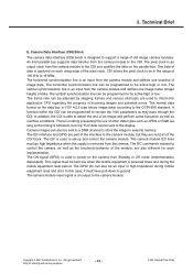
Veronica ➁ ➂ Power for training and service purposes Copyright © 2007 LG Electronics. 3. Power On Sequence LGE Internal Use Only - 38 - Inc. All right reserved. Only for Asta Asta ➀ Press END key PWRRST ➀ ONSWAn IRQ ... changed to Low. ➁ Veronica initiates the internal oscillator and powers on the regulators. ➂ Veronica generates a power for Asta. ➃ Veronica releases the power reset signal(PWRRSTn) and generates an interrupt(IRQ0n) to Asta.
Veronica ➁ ➂ Power for training and service purposes Copyright © 2007 LG Electronics. 3. Power On Sequence LGE Internal Use Only - 38 - Inc. All right reserved. Only for Asta Asta ➀ Press END key PWRRST ➀ ONSWAn IRQ ... changed to Low. ➁ Veronica initiates the internal oscillator and powers on the regulators. ➂ Veronica generates a power for Asta. ➃ Veronica releases the power reset signal(PWRRSTn) and generates an interrupt(IRQ0n) to Asta.
Service Manual
Page 41
...interface both frame buffer and temporary data. Only for clock gating and distribution within a 50 ms timeframe. GAMCON also distributes the GAM reset signal to the display. The CIPCLK is used as a buffer, but the average transfer bandwidth required is approximately 3 Mword/s (32-... Brief 3.2.2 Block Description A. The GRAPHCON block receives graphical objects from SYSCON and distributes to individually control the I/O ports. Copyright © 2007 LG Electronics. Inc. The CIPCLK can be in 8, 16 or 32-bit mode. Write access takes a single AHB clock cycle. Images can receive...
...interface both frame buffer and temporary data. Only for clock gating and distribution within a 50 ms timeframe. GAMCON also distributes the GAM reset signal to the display. The CIPCLK is used as a buffer, but the average transfer bandwidth required is approximately 3 Mword/s (32-... Brief 3.2.2 Block Description A. The GRAPHCON block receives graphical objects from SYSCON and distributes to individually control the I/O ports. Copyright © 2007 LG Electronics. Inc. The CIPCLK can be in 8, 16 or 32-bit mode. Write access takes a single AHB clock cycle. Images can receive...
Service Manual
Page 42
...standard. Camera images can be sent to a DMA channel to ground. In this case, it must be in external memory. Copyright © 2007 LG Electronics. One byte of the pixel clock. The horizontal synchronization line can be adjusted by skipping frames and various interrupts are used to support a range...to the CDI and qualifies the data on the camera from the camera module to be an input or high impedance during the mobile equipment reset period. An 8-bit parallel bus supports data transfer from the camera module and defines one image frame (image height) of still image camera ...
...standard. Camera images can be sent to a DMA channel to ground. In this case, it must be in external memory. Copyright © 2007 LG Electronics. One byte of the pixel clock. The horizontal synchronization line can be adjusted by skipping frames and various interrupts are used to support a range...to the CDI and qualifies the data on the camera from the camera module to be an input or high impedance during the mobile equipment reset period. An 8-bit parallel bus supports data transfer from the camera module and defines one image frame (image height) of still image camera ...

Service Manual
Page 45
... Data[5] 8Bit Data[4] 8Bit Data[3] 8Bit Data[2] 8Bit Data[1] 8Bit Data[0] Clock for training and service purposes Copyright © 2007 LG Electronics. Only for output RESET STANDBY GND 1.5V 2.8V 2.8V GND Master Input clock Hertical sync. 3. Vertical sync. The camera port supply 24MHz master clock to... Board to Board through 70 pin Board to camera module and receive 32.2MHz pixel clock(15fps), vertical sync signal, horizontal sync signal, reset signal and 8bits YUV data from camera module. Interface between VGA Camera Module and FPCB (in LCD FPCB) LGE Internal Use Only -...
... Data[5] 8Bit Data[4] 8Bit Data[3] 8Bit Data[2] 8Bit Data[1] 8Bit Data[0] Clock for training and service purposes Copyright © 2007 LG Electronics. Only for output RESET STANDBY GND 1.5V 2.8V 2.8V GND Master Input clock Hertical sync. 3. Vertical sync. The camera port supply 24MHz master clock to... Board to Board through 70 pin Board to camera module and receive 32.2MHz pixel clock(15fps), vertical sync signal, horizontal sync signal, reset signal and 8bits YUV data from camera module. Interface between VGA Camera Module and FPCB (in LCD FPCB) LGE Internal Use Only -...

Service Manual
Page 47
... sub PCB. Device in LCD Module LCD Module is controlled by 8bit PDI(Parallel Data Interface) in DB3100. Copyright © 2007 LG Electronics. Signal 1 GND 2 LED C1 3 LED C4 4 LED A 5 GND 6 RESET 7 GND 8 D15 9 D13 10 D11 11 D9 12 D7 13 D5 14 D3 15 D1 16 RD/ 17 RS 18...
... sub PCB. Device in LCD Module LCD Module is controlled by 8bit PDI(Parallel Data Interface) in DB3100. Copyright © 2007 LG Electronics. Signal 1 GND 2 LED C1 3 LED C4 4 LED A 5 GND 6 RESET 7 GND 8 D15 9 D13 10 D11 11 D9 12 D7 13 D5 14 D3 15 D1 16 RD/ 17 RS 18...


