Service Manual
Page 5
... Signal Processing Electrical Erasable Programmable Read-Only Memory Electrostatic Discharge Flexible Printed Circuit Board Gaussian Minimum Shift Keying General Purpose Interface Bus Global System for Mobile Communications International Portable User Identity Intermediate Frequency Liquid Crystal Display Low Drop Output Light Emitting Diode Offset Phase Locked Loop - 4-
... Signal Processing Electrical Erasable Programmable Read-Only Memory Electrostatic Discharge Flexible Printed Circuit Board Gaussian Minimum Shift Keying General Purpose Interface Bus Global System for Mobile Communications International Portable User Identity Intermediate Frequency Liquid Crystal Display Low Drop Output Light Emitting Diode Offset Phase Locked Loop - 4-
Service Manual
Page 15
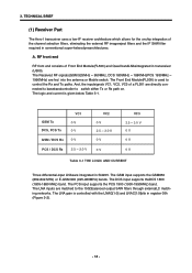
... integrated in register 05h (Figure 3-2). - 14 - The DCS input supports theDCS 1800 (1805-1880 MHz) band. The LNA inputs are fed into the antenna or Mobile switch. The LNA gain is controlled with the LNAG[1:0] and LNAC[1:0]bits in SI4205. The Front End Module(FL500) is given below Table 3-1. The PCS...
... integrated in register 05h (Figure 3-2). - 14 - The DCS input supports theDCS 1800 (1805-1880 MHz) band. The LNA inputs are fed into the antenna or Mobile switch. The LNA gain is controlled with the LNAG[1:0] and LNAC[1:0]bits in SI4205. The Front End Module(FL500) is given below Table 3-1. The PCS...
Service Manual
Page 46
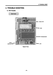
TECHNICAL BRIEF Mobile SW FEM TRANCEIVER LDO - 45 - 4. TROUBLE SHOOTING 4.1 RX Trouble TEST POINT 13Mhz OSCILLATOR Figure 4-1(a) 3.
TECHNICAL BRIEF Mobile SW FEM TRANCEIVER LDO - 45 - 4. TROUBLE SHOOTING 4.1 RX Trouble TEST POINT 13Mhz OSCILLATOR Figure 4-1(a) 3.
Service Manual
Page 47
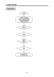
TROUBLE SHOOTING Checking Flow START HP8960 : Test mode 62 CH, 7 level setting (TCH) 62CH, -60dBm setting (BCCH) Spectrum analyzer setting Oscilloscope setting Check regulator circuit Check VCTCXO Check FEM & Mobile SW Check RX IQ Redownload SW or Do calibration again - 46 - 4 .
TROUBLE SHOOTING Checking Flow START HP8960 : Test mode 62 CH, 7 level setting (TCH) 62CH, -60dBm setting (BCCH) Spectrum analyzer setting Oscilloscope setting Check regulator circuit Check VCTCXO Check FEM & Mobile SW Check RX IQ Redownload SW or Do calibration again - 46 - 4 .
Service Manual
Page 49
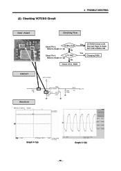
Refer to check ANT SW & Mobile SW Yes Changing X500 Check U101, PMIC CIRCUIT Waveform 100 R514 2V75_VVCXO X500 3 OUT VCONT 1 1 4 VCC C536 22u 2 GNO 13MHz C538 1000p R516 15K AFC Graph 4-1(a) Graph 4-1(b) - 48 - Refer to Graph 4-1 (a) No Yes VCTCXO Circuit is OK See next Page to Graph 4-1 (b) No Check Pin 4. 2.7V OK? TROUBLE SHOOTING (2) Checking VCTCXO Circuit TEST POINT Checking Flow Check Pin 3. 13 MHz O.K? 4 .
Refer to check ANT SW & Mobile SW Yes Changing X500 Check U101, PMIC CIRCUIT Waveform 100 R514 2V75_VVCXO X500 3 OUT VCONT 1 1 4 VCC C536 22u 2 GNO 13MHz C538 1000p R516 15K AFC Graph 4-1(a) Graph 4-1(b) - 48 - Refer to Graph 4-1 (a) No Yes VCTCXO Circuit is OK See next Page to Graph 4-1 (b) No Check Pin 4. 2.7V OK? TROUBLE SHOOTING (2) Checking VCTCXO Circuit TEST POINT Checking Flow Check Pin 3. 13 MHz O.K? 4 .

Service Manual
Page 50
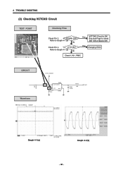
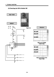
(3) Checking FEM & Mobile SW TEST POINT 4 . TROUBLE SHOOTING CIRCUIT TP502 TP501 TP500 C500 NA C502 NA C503 NA Figure 4-5 C512 2.2p Waveform KMS-507 SW500 ANT G2 G1 RF C543 22p L550 1.8nH 9 11 FL500 ANT LMSP7CHA-158 14 VC2 16 7 VC3 VC1 GSM_RX1 1 GSM_RX2 2 3 DCS_RX1 DCS_RX2 4 PCS_RX1 5 6 PCS_RX2 DCS_PCS_TX 15 17 GND3 GND1 GSM_TX GND4 GND2 12 13 19 C517 10nH C535 270p C537 270p C539 270p R512 0 R515 0 R517 0 ANT_SW3 GPO_10 ANT_SW2 GPO_11 ANT_SW1 GPO_9 FEM Control GSM & DCS Graph 4-3(a) - 49 - FEM Control PCS Graph 4-3(b)
(3) Checking FEM & Mobile SW TEST POINT 4 . TROUBLE SHOOTING CIRCUIT TP502 TP501 TP500 C500 NA C502 NA C503 NA Figure 4-5 C512 2.2p Waveform KMS-507 SW500 ANT G2 G1 RF C543 22p L550 1.8nH 9 11 FL500 ANT LMSP7CHA-158 14 VC2 16 7 VC3 VC1 GSM_RX1 1 GSM_RX2 2 3 DCS_RX1 DCS_RX2 4 PCS_RX1 5 6 PCS_RX2 DCS_PCS_TX 15 17 GND3 GND1 GSM_TX GND4 GND2 12 13 19 C517 10nH C535 270p C537 270p C539 270p R512 0 R515 0 R517 0 ANT_SW3 GPO_10 ANT_SW2 GPO_11 ANT_SW1 GPO_9 FEM Control GSM & DCS Graph 4-3(a) - 49 - FEM Control PCS Graph 4-3(b)
Service Manual
Page 51
... No VC2 :Low VC3 :Low Yes Check RF Level of FL500.1 (for GSM) & FL500.3 (for DCS) & FL500.5 (for PCS) Pin1 : ~ -62dBm No n 3,5 : ~ -63dB Yes FEM & Mobile SW is OK See next Page to check Rx IQ Signal Changing SW500 Changing SW500 Changing the board Changing FL500 For this RF Level test...
... No VC2 :Low VC3 :Low Yes Check RF Level of FL500.1 (for GSM) & FL500.3 (for DCS) & FL500.5 (for PCS) Pin1 : ~ -62dBm No n 3,5 : ~ -63dB Yes FEM & Mobile SW is OK See next Page to check Rx IQ Signal Changing SW500 Changing SW500 Changing the board Changing FL500 For this RF Level test...

Service Manual
Page 53
4 . TROUBLE SHOOTING 4.2 TX Trouble TEST POINT 13Mhz OSCILLATOR Mobile SW FEM TRANCEIVER LDO PAM - 52 -
4 . TROUBLE SHOOTING 4.2 TX Trouble TEST POINT 13Mhz OSCILLATOR Mobile SW FEM TRANCEIVER LDO PAM - 52 -
Service Manual
Page 54
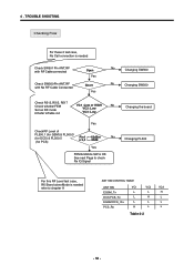
Checking Flow START HP8960 : Test mode 62 CH, 7 level setting (TCH) 62CH, -60dBm setting (BCCH) Spectrum analyzer setting Oscilloscope setting Check regulator circuit Check VCTCXO Check FEM & Mobile SW Check PAM contral signal Check TX IQ Redownload SW or Do calibration again 4 . TROUBLE SHOOTING - 53 -
Checking Flow START HP8960 : Test mode 62 CH, 7 level setting (TCH) 62CH, -60dBm setting (BCCH) Spectrum analyzer setting Oscilloscope setting Check regulator circuit Check VCTCXO Check FEM & Mobile SW Check PAM contral signal Check TX IQ Redownload SW or Do calibration again 4 . TROUBLE SHOOTING - 53 -
Service Manual
Page 56
Yes Refer to check ANT SW & Mobile SW Changing X500 2V75_VVCXO X500 3 OUT VCONT 1 1 4 VCC C536 22u 2 GNO 13MHz C538 1000p R516 15K AFC Graph 4-1(a) Graph 4-1(b) - 55 - Refer to Graph 4-1 (a) No Check U101, PMIC VCTCXO Circuit is OK See next Page to Graph 4-1 (b) No Yes Check Pin 4. 2.7V OK? TROUBLE SHOOTING TEST POINT CIRCUIT Waveform 100 R514 Checking Flow Check Pin 3. 13 MHz O.K? (2) Checking VCTCXO Circuit 4 .
Yes Refer to check ANT SW & Mobile SW Changing X500 2V75_VVCXO X500 3 OUT VCONT 1 1 4 VCC C536 22u 2 GNO 13MHz C538 1000p R516 15K AFC Graph 4-1(a) Graph 4-1(b) - 55 - Refer to Graph 4-1 (a) No Check U101, PMIC VCTCXO Circuit is OK See next Page to Graph 4-1 (b) No Yes Check Pin 4. 2.7V OK? TROUBLE SHOOTING TEST POINT CIRCUIT Waveform 100 R514 Checking Flow Check Pin 3. 13 MHz O.K? (2) Checking VCTCXO Circuit 4 .
Service Manual
Page 57
TROUBLE SHOOTING (3) Checking Ant SW & Mobile SW - 56 - 4 .
TROUBLE SHOOTING (3) Checking Ant SW & Mobile SW - 56 - 4 .
Service Manual
Page 80
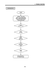
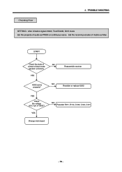
Checking Flow 4 . NO Resolder or replace U202 YES Check the voltage at 5,7 pin of mobile as PRBS or continuous wave. Set the receiving volume of U202? TROUBLE SHOOTING SETTING : After initialize Agilent 8960, Test EGSM, DCS mode Set the property of dual mode speaker (receiver) YES Reassemble receiver U202 works properly? YES Change main board NO Resolder R111, R114, C139, C140, C141 - 79 - START Check the state of NO contact of audio as Max.
Checking Flow 4 . NO Resolder or replace U202 YES Check the voltage at 5,7 pin of mobile as PRBS or continuous wave. Set the receiving volume of U202? TROUBLE SHOOTING SETTING : After initialize Agilent 8960, Test EGSM, DCS mode Set the property of dual mode speaker (receiver) YES Reassemble receiver U202 works properly? YES Change main board NO Resolder R111, R114, C139, C140, C141 - 79 - START Check the state of NO contact of audio as Max.
Service Manual
Page 120
... TAPE 3 ACGM00 COVER ASSY,REAR 4 MCJN00 COVER,REAR 4 MTAB TAPE,PROTECTION 4 MTAZ00 TAPE 3 AKAZ KEYPAD ASSY 3 GMEY00 SCREW MACHINE,BIND 3 GMZZ00 SCREW MACHINE 3 MCCF00 CAP,MOBILE SWITCH 3 MCCH00 CAP,SCREW 3 MLAK LABEL,MODEL 5 ADCA00 DOME ASSY,METAL 5 MGAD00 GASKET,SHIELD FORM 5 MTAC00 TAPE,SHIELD 5 MTAC01 TAPE,SHIELD 5 MTAZ00 TAPE Part Number...
... TAPE 3 ACGM00 COVER ASSY,REAR 4 MCJN00 COVER,REAR 4 MTAB TAPE,PROTECTION 4 MTAZ00 TAPE 3 AKAZ KEYPAD ASSY 3 GMEY00 SCREW MACHINE,BIND 3 GMZZ00 SCREW MACHINE 3 MCCF00 CAP,MOBILE SWITCH 3 MCCH00 CAP,SCREW 3 MLAK LABEL,MODEL 5 ADCA00 DOME ASSY,METAL 5 MGAD00 GASKET,SHIELD FORM 5 MTAC00 TAPE,SHIELD 5 MTAC01 TAPE,SHIELD 5 MTAZ00 TAPE Part Number...

