User Manual
Page 2
... by the third digit in the manual revision number. Manual updates are represented by the purchaser for backup purposes. Product Name: ASUS P/I-P55T2P4 Manual Revision: 3.11 Release Date: May 1997 II ASUS P/I-P55T2P4 User's Manual Specifications are both printed on the board itself. Products mentioned in this manual are mentioned for a particular purpose. The...
... by the third digit in the manual revision number. Manual updates are represented by the purchaser for backup purposes. Product Name: ASUS P/I-P55T2P4 Manual Revision: 3.11 Release Date: May 1997 II ASUS P/I-P55T2P4 User's Manual Specifications are both printed on the board itself. Products mentioned in this manual are mentioned for a particular purpose. The...
User Manual
Page 3
....tw Technical Support: Fax: 886-2-895-9254 BBS: 886-2-896-4667 Email: tsd@asus.com.tw WWW: http://www.asus.com.tw/ Gopher: gopher.asus.com.tw FTP: ftp.asus.com.tw/pub/ASUS ASUS COMPUTER INTERNATIONAL Marketing Info: Address: 721 Charcot Avenue, San Jose, CA 95131, USA Telephone: ...usa@asus.com.tw ASUS COMPUTER GmbH Marketing Info: Address: Harkort Str. 25, 40880 Ratingen, BRD, Germany Telephone: 49-2102-445011 Fax: 49-2102-442066 Email: info-ger@asus.com.tw Technical Support: BBS: 49-2102-448690 Email: tsd-ger@asus.com.tw ASUS P/I-P55T2P4 User's Manual III ASUS CONTACT ...
....tw Technical Support: Fax: 886-2-895-9254 BBS: 886-2-896-4667 Email: tsd@asus.com.tw WWW: http://www.asus.com.tw/ Gopher: gopher.asus.com.tw FTP: ftp.asus.com.tw/pub/ASUS ASUS COMPUTER INTERNATIONAL Marketing Info: Address: 721 Charcot Avenue, San Jose, CA 95131, USA Telephone: ...usa@asus.com.tw ASUS COMPUTER GmbH Marketing Info: Address: Harkort Str. 25, 40880 Ratingen, BRD, Germany Telephone: 49-2102-445011 Fax: 49-2102-442066 Email: info-ger@asus.com.tw Technical Support: BBS: 49-2102-448690 Email: tsd-ger@asus.com.tw ASUS P/I-P55T2P4 User's Manual III ASUS CONTACT ...
User Manual
Page 4
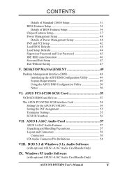
CONTENTS I -P55T2P4 User's Manual Central Processing Unit (CPU 15 4. External Connectors 19 Power Connection Procedures 25 IV. Expansion Cards 16 Expansion Card Installation Procedure 16 Assigning IRQs ... 12 TAG SRAM Upgrade 12 DRAM Memory Installation Procedures 13 Static RAM (SRAM) for Level 2 (External) Cache 14 Compatible Cache Modules for ISA Cards 17 ASUS MediaBus Card 18 5. Jumpers 6 Jumper Settings 7 Cyrix CPU Identification 11 2. BIOS Setup 29 Load Defaults 30 Standard CMOS Setup 30 IV...
CONTENTS I -P55T2P4 User's Manual Central Processing Unit (CPU 15 4. External Connectors 19 Power Connection Procedures 25 IV. Expansion Cards 16 Expansion Card Installation Procedure 16 Assigning IRQs ... 12 TAG SRAM Upgrade 12 DRAM Memory Installation Procedures 13 Static RAM (SRAM) for Level 2 (External) Cache 14 Compatible Cache Modules for ISA Cards 17 ASUS MediaBus Card 18 5. Jumpers 6 Jumper Settings 7 Cyrix CPU Identification 11 2. BIOS Setup 29 Load Defaults 30 Standard CMOS Setup 30 IV...
User Manual
Page 5
...SC200 54 Setting the INT Assignment 55 Terminator Settings 55 SCSI ID Numbers 56 VII. Windows 95 Audio Software (with optional ASUS I-A16C Audio Card Bundle Only) IX. CONTENTS Details of Standard CMOS Setup 31 BIOS Features Setup 34 Details of BIOS Features...IDE HDD Auto Detection 46 Save and Exit Setup 47 Exit Without Saving 47 V. ASUS I-A16C Audio Card 57 ASUS I -P55T2P4 User's Manual V DOS 3.1 & Windows 3.1x Audio Software (with optional ASUS I-A16C Audio Card Bundle Only) ASUS P/I -A16C Audio Features 57 Unpacking and Handling Precautions 57 Layout and Connectors 58 ...
...SC200 54 Setting the INT Assignment 55 Terminator Settings 55 SCSI ID Numbers 56 VII. Windows 95 Audio Software (with optional ASUS I-A16C Audio Card Bundle Only) IX. CONTENTS Details of Standard CMOS Setup 31 BIOS Features Setup 34 Details of BIOS Features...IDE HDD Auto Detection 46 Save and Exit Setup 47 Exit Without Saving 47 V. ASUS I-A16C Audio Card 57 ASUS I -P55T2P4 User's Manual V DOS 3.1 & Windows 3.1x Audio Software (with optional ASUS I-A16C Audio Card Bundle Only) ASUS P/I -A16C Audio Features 57 Unpacking and Handling Precautions 57 Layout and Connectors 58 ...
User Manual
Page 6
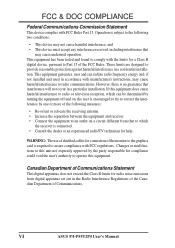
... help. If this equipment does cause harmful interference to radio or television reception, which the receiver is no guarantee that may cause undesired operation. VI ASUS P/I-P55T2P4 User's Manual This equipment generates, uses and can be determined by turning the equipment off and on, the user is required to assure compliance with...
... help. If this equipment does cause harmful interference to radio or television reception, which the receiver is no guarantee that may cause undesired operation. VI ASUS P/I-P55T2P4 User's Manual This equipment generates, uses and can be determined by turning the equipment off and on, the user is required to assure compliance with...
User Manual
Page 7
... this product III. Installation: Instructions on the included support software VI. Windows 95: Audio Software Manual (with ASUS I -P55T2P4 User's Manual 1 Features: Information and specifications concerning this manual is organized This manual is complete. ASUS SCSI: Installation of an optional ASUS SCSI cards VII. DOS/Win3.1x: Audio Software Manual (with mounting bracket Optional...
... this product III. Installation: Instructions on the included support software VI. Windows 95: Audio Software Manual (with ASUS I -P55T2P4 User's Manual 1 Features: Information and specifications concerning this manual is organized This manual is complete. ASUS SCSI: Installation of an optional ASUS SCSI cards VII. DOS/Win3.1x: Audio Software Manual (with mounting bracket Optional...
User Manual
Page 8
... also supported without an external card. The Japanese "Floppy 3 mode" (3.5" 1.2MB) floppy standard is also supported. 2 ASUS P/I -P55T2P4 is carefully designed for an optional high-performance expansion card which allows hardware to communicate within a standard protocol creating a higher ..., or 64MB to form a memory size between 8MB to 512KB, or 512KB onboard Pipelined Burst SRAM. Two floppy drives of the ASUS Motherboard The ASUS P/I -P55T2P4 User's Manual UART2 can detect multi-bit memory errors and correct 1bit memory errors. • Desktop Management Interface (DMI): Supports DMI...
... also supported without an external card. The Japanese "Floppy 3 mode" (3.5" 1.2MB) floppy standard is also supported. 2 ASUS P/I -P55T2P4 is carefully designed for an optional high-performance expansion card which allows hardware to communicate within a standard protocol creating a higher ..., or 64MB to form a memory size between 8MB to 512KB, or 512KB onboard Pipelined Burst SRAM. Two floppy drives of the ASUS Motherboard The ASUS P/I -P55T2P4 User's Manual UART2 can detect multi-bit memory errors and correct 1bit memory errors. • Desktop Management Interface (DMI): Supports DMI...
User Manual
Page 9
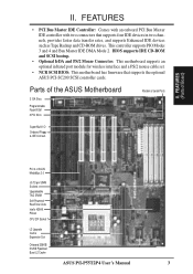
... Enhanced IDE devices such as Tape Backup and CD-ROM drives. FEATURES (Parts of the ASUS Motherboard 3 ISA Slots Programmable Flash ROM 3 PCI Slots Parallel & Serial Ports Super Multi-I -P55T2P4 User's Manual 3 FEATURES • PCI Bus Master IDE Controller: Comes with an onboard PCI... Bus Master IDE controller with two connectors that supports the optional ASUS PCI-SC200 SCSI controller cards. Parts of Board) II. PCI 4 or ASUS MediaBus 2.0 (4) 72-pin ...
... Enhanced IDE devices such as Tape Backup and CD-ROM drives. FEATURES (Parts of the ASUS Motherboard 3 ISA Slots Programmable Flash ROM 3 PCI Slots Parallel & Serial Ports Super Multi-I -P55T2P4 User's Manual 3 FEATURES • PCI Bus Master IDE Controller: Comes with an onboard PCI... Bus Master IDE controller with two connectors that supports the optional ASUS PCI-SC200 SCSI controller cards. Parts of Board) II. PCI 4 or ASUS MediaBus 2.0 (4) 72-pin ...
User Manual
Page 10
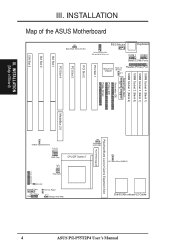
INSTALLATION (Map of the ASUS Motherboard ISA Slot 2 ISA Slot 3 JP2 Boot Block Write (Dis/En) PS/2 Mouse Keyboard Universal Serial Bus (Reserved for future use) COM 1 COM 2 Serial (COM) Ports MULTI I/O Chipset Multi-I -P55T2P4 User's Manual INSTALLATION Map of Board) Board Power Input P9...) JP11 JP12 Case Connector Freq Ratio IDE LED Infrared Conn. CPU VCore JP20 12V Fan Power JP17 Voltage (STD/VRE) 256/512KB onboard L2 Cache 4 ASUS P/I /O (En/Dis) JP1 Parallel (Printer) Port PCI Slot 1 PCI Slot 2 PCI Slot 3 PCI Slot 4 ISA Slot 1 SIMM Socket 4 (Bank 1) SIMM ...
INSTALLATION (Map of the ASUS Motherboard ISA Slot 2 ISA Slot 3 JP2 Boot Block Write (Dis/En) PS/2 Mouse Keyboard Universal Serial Bus (Reserved for future use) COM 1 COM 2 Serial (COM) Ports MULTI I/O Chipset Multi-I -P55T2P4 User's Manual INSTALLATION Map of Board) Board Power Input P9...) JP11 JP12 Case Connector Freq Ratio IDE LED Infrared Conn. CPU VCore JP20 12V Fan Power JP17 Voltage (STD/VRE) 256/512KB onboard L2 Cache 4 ASUS P/I /O (En/Dis) JP1 Parallel (Printer) Port PCI Slot 1 PCI Slot 2 PCI Slot 3 PCI Slot 4 ISA Slot 1 SIMM Socket 4 (Bank 1) SIMM ...
User Manual
Page 11
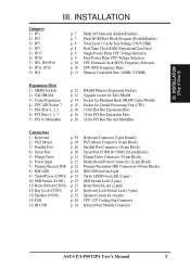
INSTALLATION Jumpers 1) JP1 2) JP2 3) JP5 4) JP7 5) JP17 6) JP20 7) JP8, JP9,JP10 8) JP11, JP12 9) JP4 p. 7 Multi-I -P55T2P4 User's Manual 5 IDE p. 22 8) IDE LED p. 22 9) Turbo/Power (CON1) p. 23 10) SMI Switch (CON1) p. 23 11) Reset Switch (CON1) p....) SMI Switch Lead (2-pins) Reset Switch Lead (2-pins) Keyboard Lock Switch Lead (5-pins) Speaker Connector (4-pins) CPU 12V Cooling Fan Connector Infrared Port Module Connector ASUS P/I /O Selection (Enable/Disable) p. 7 Flash ROM Boot Block Program (Disable/Enable) p. 8 Total Level 2 Cache Size Setting (256/512KB) p. 8 Real Time Clock...
INSTALLATION Jumpers 1) JP1 2) JP2 3) JP5 4) JP7 5) JP17 6) JP20 7) JP8, JP9,JP10 8) JP11, JP12 9) JP4 p. 7 Multi-I -P55T2P4 User's Manual 5 IDE p. 22 8) IDE LED p. 22 9) Turbo/Power (CON1) p. 23 10) SMI Switch (CON1) p. 23 11) Reset Switch (CON1) p....) SMI Switch Lead (2-pins) Reset Switch Lead (2-pins) Keyboard Lock Switch Lead (5-pins) Speaker Connector (4-pins) CPU 12V Cooling Fan Connector Infrared Port Module Connector ASUS P/I /O Selection (Enable/Disable) p. 7 Flash ROM Boot Block Program (Disable/Enable) p. 8 Total Level 2 Cache Size Setting (256/512KB) p. 8 Real Time Clock...
User Manual
Page 12
... IC chips, leads, or circuitry. 3. tions of following steps: 1. The jumper settings will also be sharing pins from other components against damage from the system. 6 ASUS P/I-P55T2P4 User's Manual Pin 1 Pin 1 tively. Pin 1 for Open (Off). For manufacturing simplicity, the jumpers may be shown graphically such as diagramed. Use the diagrams in...
... IC chips, leads, or circuitry. 3. tions of following steps: 1. The jumper settings will also be sharing pins from other components against damage from the system. 6 ASUS P/I-P55T2P4 User's Manual Pin 1 Pin 1 tively. Pin 1 for Open (Off). For manufacturing simplicity, the jumpers may be shown graphically such as diagramed. Use the diagrams in...
User Manual
Page 13
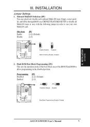
...with the following jumper in the Enabled position. Selections Enable Disable JP1 [1-2] (Default) [2-3] JP1 1 2 3 Enable (Default) JP1 1 2 3 Disabled Multi I -P55T2P4 User's Manual 7 Onboard Multi-I/O Selection (JP1) You can selectively disable each onboard Multi-I/O item (floppy, serial, parallel, and IrDA) through BIOS (see CHIPSET FEATURES .../O card. Programming Disabled Enabled JP2 [1-2] (Default) [2-3] JP2 123 Disabled (Default) JP2 123 Enabled Boot Block Programming (Disable / Enable) ASUS P/I /O Setting (Enable / Disable) 2. III. INSTALLATION Jumper Settings 1.
...with the following jumper in the Enabled position. Selections Enable Disable JP1 [1-2] (Default) [2-3] JP1 1 2 3 Enable (Default) JP1 1 2 3 Disabled Multi I -P55T2P4 User's Manual 7 Onboard Multi-I/O Selection (JP1) You can selectively disable each onboard Multi-I/O item (floppy, serial, parallel, and IrDA) through BIOS (see CHIPSET FEATURES .../O card. Programming Disabled Enabled JP2 [1-2] (Default) [2-3] JP2 123 Disabled (Default) JP2 123 Enabled Boot Block Programming (Disable / Enable) ASUS P/I /O Setting (Enable / Disable) 2. III. INSTALLATION Jumper Settings 1.
User Manual
Page 14
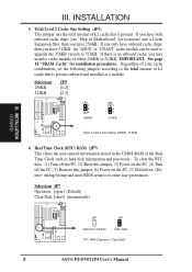
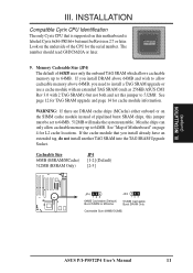
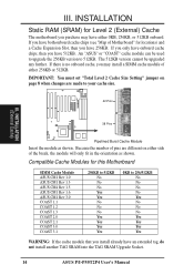
... L2 cache that is present. Selections JP7 Operation [open] (Default) Clear Data [short] (momentarily) JP7 JP7 Operation (Default) Clear Data RTC RAM (Operation / Clear Data) 8 ASUS P/I-P55T2P4 User's Manual III. INSTALLATION 3. An "ASUS" or "COAST" cache module can be used to upgrade the 256KB version to 512KB.
... L2 cache that is present. Selections JP7 Operation [open] (Default) Clear Data [short] (momentarily) JP7 JP7 Operation (Default) Clear Data RTC RAM (Operation / Clear Data) 8 ASUS P/I-P55T2P4 User's Manual III. INSTALLATION 3. An "ASUS" or "COAST" cache module can be used to upgrade the 256KB version to 512KB.
User Manual
Page 15
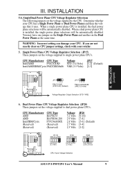
... 2.8 Volts 2.7 Volts 2.5 Volts JP20 [9-10] [7-8] [5-6] (Default) [3-4] [1-2] [9-10] JP20 K6-PR233 (3.2 Volts) [7-8] JP20 K6-PR166,200 (2.9 Volts) [5-6] JP20 P55C/6x86MX (2.8V) (Default) CPU Vcore Voltage Selection ASUS P/I-P55T2P4 User's Manual 9 INSTALLATION 5-6. When a dual power plane CPU is installed, the dual power plane selections will be automatically disabled. Determine whether your CPU has a Single...
... 2.8 Volts 2.7 Volts 2.5 Volts JP20 [9-10] [7-8] [5-6] (Default) [3-4] [1-2] [9-10] JP20 K6-PR233 (3.2 Volts) [7-8] JP20 K6-PR166,200 (2.9 Volts) [5-6] JP20 P55C/6x86MX (2.8V) (Default) CPU Vcore Voltage Selection ASUS P/I-P55T2P4 User's Manual 9 INSTALLATION 5-6. When a dual power plane CPU is installed, the dual power plane selections will be automatically disabled. Determine whether your CPU has a Single...
User Manual
Page 16
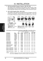
... clock generator what frequency to send to BUS Frequency Ratio (JP11, JP12) These jumpers set together with the Cyrix PR166+ installed on this motherboard. 10 ASUS P/I-P55T2P4 User's Manual JP8 JP9 JP10 JP8 JP9 JP10 JP8 JP9 JP10 JP8 JP9 JP10 JP8 JP9 JP10 1 1 1 1 2 2 2 2 3 3 3 3 50MHz 55MHz 60MHz 66MHz CPU External Clock (BUS...
... clock generator what frequency to send to BUS Frequency Ratio (JP11, JP12) These jumpers set together with the Cyrix PR166+ installed on this motherboard. 10 ASUS P/I-P55T2P4 User's Manual JP8 JP9 JP10 JP8 JP9 JP10 JP8 JP9 JP10 JP8 JP9 JP10 JP8 JP9 JP10 1 1 1 1 2 2 2 2 3 3 3 3 50MHz 55MHz 60MHz 66MHz CPU External Clock (BUS...
User Manual
Page 17
...) JP4 [1-2] (Default) [2-3] JP4 123 64MB Cacheable (Default) Burst SRAM or MCache JP4 123 512MB Cacheable Burst SRAM Only Cacheable Size (64MB/512MB) ASUS P/I-P55T2P4 User's Manual 11 See "Map of Motherboard" on the SIMM cache module instead of 64MB uses only the onboard TAG SRAM which allows cacheable memory... up to 64MB. If you need to install a TAG SRAM upgrade or use a cache module with an extended TAG SRAM (such as 256KB ASUS CM1 Rev 3.0 with 2 TAG SRAM's) but must be Revision 2.7 or later. WARNING: If there are DRAM cache chips (MCache) either onboard or ...
...) JP4 [1-2] (Default) [2-3] JP4 123 64MB Cacheable (Default) Burst SRAM or MCache JP4 123 512MB Cacheable Burst SRAM Only Cacheable Size (64MB/512MB) ASUS P/I-P55T2P4 User's Manual 11 See "Map of Motherboard" on the SIMM cache module instead of 64MB uses only the onboard TAG SRAM which allows cacheable memory... up to 64MB. If you need to install a TAG SRAM upgrade or use a cache module with an extended TAG SRAM (such as 256KB ASUS CM1 Rev 3.0 with 2 TAG SRAM's) but must be Revision 2.7 or later. WARNING: If there are DRAM cache chips (MCache) either onboard or ...
User Manual
Page 18
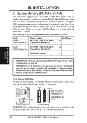
... more than 24 chips per module. You must have an extended tag, do not install another TAG SRAM into the TAG SRAM Upgrade Socket. 12 ASUS P/I-P55T2P4 User's Manual Notch Indention Insert one 16K8 or 32K8 SRAM chip as the "Notch." TAG SRAM Upgrade: The purpose of the memory subsystem and will...
... more than 24 chips per module. You must have an extended tag, do not install another TAG SRAM into the TAG SRAM Upgrade Socket. 12 ASUS P/I-P55T2P4 User's Manual Notch Indention Insert one 16K8 or 32K8 SRAM chip as the "Notch." TAG SRAM Upgrade: The purpose of the memory subsystem and will...
User Manual
Page 19
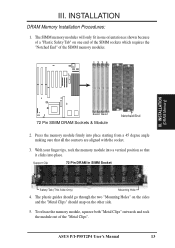
ASUS P/I-P55T2P4 User's Manual 13 The SIMM memory modules will only fit in SIMM Socket Safety Tab (This Side Only) Mounting Hole 4. Support Clip 72 Pin DRAM ...
ASUS P/I-P55T2P4 User's Manual 13 The SIMM memory modules will only fit in SIMM Socket Safety Tab (This Side Only) Mounting Hole 4. Support Clip 72 Pin DRAM ...
User Manual
Page 20
... is no onboard cache, you install already have 256KB. Because the number of Motherboard" for this Motherboard SIMM Cache Module ASUS CM1 Rev 1.0 ASUS CM1 Rev 1.3 ASUS CM4 Rev 1.5 ASUS CM1 Rev 1.6 ASUS CM1 Rev 3.0 COAST 1.1 COAST 1.2 COAST 1.3 COAST 2.0 COAST 2.1 COAST 3.0 COAST 3.1 256KB to 512KB No No...upgraded any further. If you have an extended tag, do not install another TAG SRAM into the TAG SRAM Upgrade Socket. 14 ASUS P/I-P55T2P4 User's Manual IMPORTANT: You must set "Total Level 2 Cache Size Setting" jumper on either 256KB or 512KB. INSTALLATION (External Cache...
... is no onboard cache, you install already have 256KB. Because the number of Motherboard" for this Motherboard SIMM Cache Module ASUS CM1 Rev 1.0 ASUS CM1 Rev 1.3 ASUS CM4 Rev 1.5 ASUS CM1 Rev 1.6 ASUS CM1 Rev 3.0 COAST 1.1 COAST 1.2 COAST 1.3 COAST 2.0 COAST 2.1 COAST 3.0 COAST 3.1 256KB to 512KB No No...upgraded any further. If you have an extended tag, do not install another TAG SRAM into the TAG SRAM Upgrade Socket. 14 ASUS P/I-P55T2P4 User's Manual IMPORTANT: You must set "Total Level 2 Cache Size Setting" jumper on either 256KB or 512KB. INSTALLATION (External Cache...

User Manual
Page 21
... from that corner of the square array of the four corners, the CPU will cover the face of the CPU with Pentium Processor 1 White Dot ASUS P/I-P55T2P4 User's Manual 15 WARNING: Without a fan, the CPU can overheat and cause damage to that corner. III. INSTALLATION (CPU) III. The CPU that will only...
... from that corner of the square array of the four corners, the CPU will cover the face of the CPU with Pentium Processor 1 White Dot ASUS P/I-P55T2P4 User's Manual 15 WARNING: Without a fan, the CPU can overheat and cause damage to that corner. III. INSTALLATION (CPU) III. The CPU that will only...


