Service Manual
Page 12
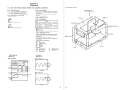
...with mark 0 are taken with a oscilloscope. Note on the conductor side. • b : Pattern from the conductor side. • x : parts mounted on Schematic Diagram: • All capacitors are taken with a VOM (Input impedance 10 MΩ). tion tolerances. • Waveforms are in Ω and 1/4 W or less...15 F03 14 F04 13 F05 12 F06 11 REC LEVEL 10 VCC • Waveforms - SECTION 5 DIAGRAMS 5-1. NOTE FOR PRINTED WIRING BOARDS AND SCHEMATIC DIAGRAMS Note on Printed Wiring Board: • X : parts extracted from the component side. • Y : parts extracted from the side which...
...with mark 0 are taken with a oscilloscope. Note on the conductor side. • b : Pattern from the conductor side. • x : parts mounted on Schematic Diagram: • All capacitors are taken with a VOM (Input impedance 10 MΩ). tion tolerances. • Waveforms are in Ω and 1/4 W or less...15 F03 14 F04 13 F05 12 F06 11 REC LEVEL 10 VCC • Waveforms - SECTION 5 DIAGRAMS 5-1. NOTE FOR PRINTED WIRING BOARDS AND SCHEMATIC DIAGRAMS Note on Printed Wiring Board: • X : parts extracted from the component side. • Y : parts extracted from the side which...
Service Manual
Page 45
... may be handled with care. DISASSEMBLY 6 4. TEST MODE 13 5. BD Board 21 7-4. Schematic Diagram - Schematic Diagram - Schematic Diagram - PANEL Section 31 7-15. OR DOTTED LINE WITH MARK ! REPLACE THESE COMPONENTS WITH SONY PARTS WHOSE PART NUMBERS APPEAR AS SHOWN IN THIS MANUAL OR IN SUPPLEMENTS PUBLISHED BY.... IC Pin Function Description 34 8. ON THE SCHEMATIC DIAGRAMS AND IN THE PARTS LIST ARE CRITICAL TO SAFE OPERATION. LES COMPOSANTS IDENTIFIÉS PAR UNE MARQUE ! NE REMPLACER CES COMPOSANTS QUE PAR DES PIÈCES SONY DONT LES NUMÉROS SONT DONNÉS ...
... may be handled with care. DISASSEMBLY 6 4. TEST MODE 13 5. BD Board 21 7-4. Schematic Diagram - Schematic Diagram - Schematic Diagram - PANEL Section 31 7-15. OR DOTTED LINE WITH MARK ! REPLACE THESE COMPONENTS WITH SONY PARTS WHOSE PART NUMBERS APPEAR AS SHOWN IN THIS MANUAL OR IN SUPPLEMENTS PUBLISHED BY.... IC Pin Function Description 34 8. ON THE SCHEMATIC DIAGRAMS AND IN THE PARTS LIST ARE CRITICAL TO SAFE OPERATION. LES COMPOSANTS IDENTIFIÉS PAR UNE MARQUE ! NE REMPLACER CES COMPOSANTS QUE PAR DES PIÈCES SONY DONT LES NUMÉROS SONT DONNÉS ...
Service Manual
Page 62
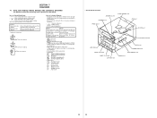
... : Pattern from the side which enables seeing. (The other layers' patterns are not indicated.) Caution: Pattern face side: (Side B) Parts face side: (Side A) Parts on Schematic Diagram: • All capacitors are indicated. Note: The components identified by mark 0 or dotted line with a VOM (Input impedance 10 MΩ). Line. • H : ...Replace only with a oscilloscope. pF: µµF 50 WV or less are in µF unless otherwise noted. NOTE FOR PRINTED WIRING BOARDS AND SCHEMATIC DIAGRAMS (In addition to normal production tolerances. • Waveforms are omitted.
... : Pattern from the side which enables seeing. (The other layers' patterns are not indicated.) Caution: Pattern face side: (Side B) Parts face side: (Side A) Parts on Schematic Diagram: • All capacitors are indicated. Note: The components identified by mark 0 or dotted line with a VOM (Input impedance 10 MΩ). Line. • H : ...Replace only with a oscilloscope. pF: µµF 50 WV or less are in µF unless otherwise noted. NOTE FOR PRINTED WIRING BOARDS AND SCHEMATIC DIAGRAMS (In addition to normal production tolerances. • Waveforms are omitted.
Service Manual
Page 64
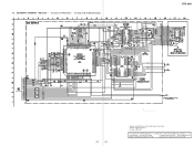
7-3. SCHEMATIC DIAGRAM - no -signal conditions. Ne les remplacer que par une pièce portant le numéro spécifié. Replace only with mark 0 are critical for IC Block Diagrams. HTC-NX1 (Page 29) 21 21 • Voltages and waveforms are dc with respect to ground under no mark : CD PLAY The components identified by mark 0 or dotted line with part number specified. BD Board - • See page 32 for Waveforms. • See page 32 for safety. Les composants identifiés par une marque 0 sont critiques pour la sécurité.
7-3. SCHEMATIC DIAGRAM - no -signal conditions. Ne les remplacer que par une pièce portant le numéro spécifié. Replace only with mark 0 are critical for IC Block Diagrams. HTC-NX1 (Page 29) 21 21 • Voltages and waveforms are dc with respect to ground under no mark : CD PLAY The components identified by mark 0 or dotted line with part number specified. BD Board - • See page 32 for Waveforms. • See page 32 for safety. Les composants identifiés par une marque 0 sont critiques pour la sécurité.
Service Manual
Page 66
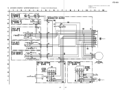
no -signal conditions. SCHEMATIC DIAGRAM - 7-5. CD MOTOR/SENSOR Section - • See page 33 for IC Block Diagram. • Voltages are dc with respect to ground under no mark : CD PLAY HTC-NX1 (Page 29) 23 23 (Page 29)
no -signal conditions. SCHEMATIC DIAGRAM - 7-5. CD MOTOR/SENSOR Section - • See page 33 for IC Block Diagram. • Voltages are dc with respect to ground under no mark : CD PLAY HTC-NX1 (Page 29) 23 23 (Page 29)
Service Manual
Page 68
SCHEMATIC DIAGRAM - Replace only with respect to ground under no-signal conditions. no mark : TAPE PLAYBACK ( ) : RECORD The components identified by mark 0 or dotted line with ... A +7.5V APB-LCH APB-RCH AGND BPB-LCH BPB-RCH A -7.5V D (Page 28) -VBIAS (-7.5V) +VBIAS (+7.5V) B-REC-RCH B-REC-LCH TC-HEAD-GND HTC-NX1 REC BIAS (R) (DECK B) REC BIAS (L) (DECK B) BIAS OSC REC BIAS -6.8 25 25 • Voltages are critical for safety. 7-7.
SCHEMATIC DIAGRAM - Replace only with respect to ground under no-signal conditions. no mark : TAPE PLAYBACK ( ) : RECORD The components identified by mark 0 or dotted line with ... A +7.5V APB-LCH APB-RCH AGND BPB-LCH BPB-RCH A -7.5V D (Page 28) -VBIAS (-7.5V) +VBIAS (+7.5V) B-REC-RCH B-REC-LCH TC-HEAD-GND HTC-NX1 REC BIAS (R) (DECK B) REC BIAS (L) (DECK B) BIAS OSC REC BIAS -6.8 25 25 • Voltages are critical for safety. 7-7.
Service Manual
Page 69
... B-SHUT A PLAY B-HALF / REC-A / REC-B B-120/70 B PALY NC E (Page 28) • Voltages are dc with respect to measure 26 26 PRINTED WIRING BOARD - SCHEMATIC DIAGRAM - HTC-NX1 7-8. LEAF SW Board - (CAPSTAN) CONTROL SWITCH DECK B PLUNGER DECK A PLUNGER (DECK A 120/70) (DECK A HALF) (DECK A REC) (DECK B HALF) (DECK B REC) (DECK B 120/70...
... B-SHUT A PLAY B-HALF / REC-A / REC-B B-120/70 B PALY NC E (Page 28) • Voltages are dc with respect to measure 26 26 PRINTED WIRING BOARD - SCHEMATIC DIAGRAM - HTC-NX1 7-8. LEAF SW Board - (CAPSTAN) CONTROL SWITCH DECK B PLUNGER DECK A PLUNGER (DECK A 120/70) (DECK A HALF) (DECK A REC) (DECK B HALF) (DECK B REC) (DECK B 120/70...
Service Manual
Page 72
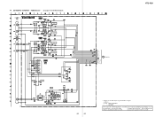
SCHEMATIC DIAGRAM - no -signal conditions. MAIN Board (2/2) - • See page 32 for Waveform. (Page 28) HTC-NX1 (Page 23) (Page 23) (Page 21) (Page 31) (Page 31) (Page 31) 29 29 • Voltages and waveforms are dc with respect to ground under no mark : CD PLAY ( ) : TAPE PLAYBACK (DECK A) [ ] : TAPE PLAYBACK (DECK B) RECORD ∗ : Impossible to measure 7-12.
SCHEMATIC DIAGRAM - no -signal conditions. MAIN Board (2/2) - • See page 32 for Waveform. (Page 28) HTC-NX1 (Page 23) (Page 23) (Page 21) (Page 31) (Page 31) (Page 31) 29 29 • Voltages and waveforms are dc with respect to ground under no mark : CD PLAY ( ) : TAPE PLAYBACK (DECK A) [ ] : TAPE PLAYBACK (DECK B) RECORD ∗ : Impossible to measure 7-12.

Service Manual
Page 74
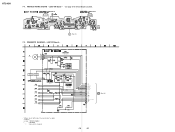
PANEL Section - (Page 29) (Page 29) (Page 29) HTC-NX1 31 31 • Voltages are dc with respect to ground under no mark : CD PLAY 7-14. no -signal conditions. SCHEMATIC DIAGRAM -
PANEL Section - (Page 29) (Page 29) (Page 29) HTC-NX1 31 31 • Voltages are dc with respect to ground under no mark : CD PLAY 7-14. no -signal conditions. SCHEMATIC DIAGRAM -


