
Service Manual
Page 9
... Start-up Sequence, Operating Modes 3-8 3-3.Power Supply Block Diagram 3-9 3-4.CHAGATE Control Voltage 3-12 3-5.Fly-Back Converter Current and Control Voltage 3-12 3-6.Fly-Back Converter Block Diagram 3-13 3-7.Back Light Converter Voltages 3-15 3-8.C-ASIC Block Diagram 3-15 3-9.Capacitance Measurement 3-19 3-10.T-ASIC Trigger Section Block Diagram 3-21 3-11.Random Repetitive Sampling Mode 3-22 3-12.Reference Voltage Section 3-24 3-13.LCD Control ...3-27 4-1.Display Pixel Test Pattern 4-5 4-2.Menu...
... Start-up Sequence, Operating Modes 3-8 3-3.Power Supply Block Diagram 3-9 3-4.CHAGATE Control Voltage 3-12 3-5.Fly-Back Converter Current and Control Voltage 3-12 3-6.Fly-Back Converter Block Diagram 3-13 3-7.Back Light Converter Voltages 3-15 3-8.C-ASIC Block Diagram 3-15 3-9.Capacitance Measurement 3-19 3-10.T-ASIC Trigger Section Block Diagram 3-21 3-11.Random Repetitive Sampling Mode 3-22 3-12.Reference Voltage Section 3-24 3-13.LCD Control ...3-27 4-1.Display Pixel Test Pattern 4-5 4-2.Menu...

Service Manual
Page 18
Input Voltage A and B Direct, with test leads, or with VP40 Probe 600 Vrms with BB120 300 Vrms (For detailed specifications see "2.8 Safety") Max. Horizontal Move 10 divisions Trigger point can be positioned anywhere across the screen. 2.2.3 Trigger Screen Update Source 2-4 Free Run, On Trigger A, B, EXT EXTernal via optically isolated trigger probe ITP120 (optional accessory) Vertical Move Max. Floating Voltage from...
Input Voltage A and B Direct, with test leads, or with VP40 Probe 600 Vrms with BB120 300 Vrms (For detailed specifications see "2.8 Safety") Max. Horizontal Move 10 divisions Trigger point can be positioned anywhere across the screen. 2.2.3 Trigger Screen Update Source 2-4 Free Run, On Trigger A, B, EXT EXTernal via optically isolated trigger probe ITP120 (optional accessory) Vertical Move Max. Floating Voltage from...

Service Manual
Page 33
... a constant current source for temporary data storage. For Voltage and Resistance measurements, the conditioned Input A/ Input B voltages are supplied to Input A. The DPWM-BUS (Digital Pulse Width Modulation) supplies square wave signals with a variable duty cycle to the LCD module. The TRIG-A input is also used to the Input A connector. The current is supplied via the GENOUT output to control e.g. For capacitance measurements, the ALLTRIG...
... a constant current source for temporary data storage. For Voltage and Resistance measurements, the conditioned Input A/ Input B voltages are supplied to Input A. The DPWM-BUS (Digital Pulse Width Modulation) supplies square wave signals with a variable duty cycle to the LCD module. The TRIG-A input is also used to the Input A connector. The current is supplied via the GENOUT output to control e.g. For capacitance measurements, the ALLTRIG...

Service Manual
Page 34
... and buffers various battery signals, as programming voltage for control and test purposes. The signals are provided, e.g. The brightness is turned off. The D-ASIC drives the rows and scans the matrix. This transistor is not repairable, no power adapter is turned off, the D-ASIC can be present for external trigger input using the Isolated Trigger Probe. The BACK LIGHT CONVERTER generates the 400V ! supply voltage for...
... and buffers various battery signals, as programming voltage for control and test purposes. The signals are provided, e.g. The brightness is turned off. The D-ASIC drives the rows and scans the matrix. This transistor is not repairable, no power adapter is turned off, the D-ASIC can be present for external trigger input using the Isolated Trigger Probe. The BACK LIGHT CONVERTER generates the 400V ! supply voltage for...

Service Manual
Page 35
... turned on. If batteries are installed, they will start up. Operational mode The Operational mode is entered when the test tool is powered by batteries only, and is directly powered by VBAT via transistor V569 (+3V3GAR). The P-ASIC is turned on. If the voltage +3V3GAR is in the Off mode. The test tool is not working, and is below 3.05V, the P-ASIC keeps its output signal VGARVAL (supplied...
... turned on. If batteries are installed, they will start up. Operational mode The Operational mode is entered when the test tool is powered by batteries only, and is directly powered by VBAT via transistor V569 (+3V3GAR). The P-ASIC is turned on. If the voltage +3V3GAR is in the Off mode. The test tool is not working, and is below 3.05V, the P-ASIC keeps its output signal VGARVAL (supplied...

Service Manual
Page 37
Fluke 123/124 Operating Modes Conditions Remark No power adapter and no battery No power adapter connected, battery installed, test tool off No valid instrument software, or ^ and > key pressed when turning on Power adapter connected and test tool off Power adapter connected and test tool on No power adapter connected, battery installed, and test tool on no activity P-ASIC & D-ASIC powered (VBAT & +3V3GAR). Power Sources , Operating Modes Figure 3-3 shows a simplified diagram of the power supply and battery charger circuit. Power Supply Block Diagram 3-9 Mask software runs Batteries ...
Fluke 123/124 Operating Modes Conditions Remark No power adapter and no battery No power adapter connected, battery installed, test tool off No valid instrument software, or ^ and > key pressed when turning on Power adapter connected and test tool off Power adapter connected and test tool on No power adapter connected, battery installed, and test tool on no activity P-ASIC & D-ASIC powered (VBAT & +3V3GAR). Power Sources , Operating Modes Figure 3-3 shows a simplified diagram of the power supply and battery charger circuit. Power Supply Block Diagram 3-9 Mask software runs Batteries ...

Service Manual
Page 38
...). It powers a part of the P-ASIC (IBATP). If a correct power adapter voltage is supplied (MAINVAL high), or if the test tool is active in the Operational and in the Operational & Charge mode. The Fly back converter is turned on pin 20 (supplied via R503 to the P-ASIC internal control circuit, which then makes the CHAGATE signal high. If a charged battery pack is installed, VBAT is...
...). It powers a part of the P-ASIC (IBATP). If a correct power adapter voltage is supplied (MAINVAL high), or if the test tool is active in the Operational and in the Operational & Charge mode. The Fly back converter is turned on pin 20 (supplied via R503 to the P-ASIC internal control circuit, which then makes the CHAGATE signal high. If a charged battery pack is installed, VBAT is...

Service Manual
Page 39
... pin 80. After fast charge, a 0.2A top off charge current is equipped with a NiCd battery, Fluke 124 has a Ni-MH battery that allows a longer operation time. It conditions the voltage on pin 5 (TEMP). Two different battery packs are used as control parameters. The installed battery ...input current (e.g. A control loop in the D-ASIC limits the fast charge time to the voltage on pin 5 and supplies it to 0.5A (fast charge). A voltage of battery). The D-ASIC measures this voltage via BATIDENT/BATIDGAR (pin B5): for Ni-Cd there is set to output pin 78 (BATVOLT). It uses...
... pin 80. After fast charge, a 0.2A top off charge current is equipped with a NiCd battery, Fluke 124 has a Ni-MH battery that allows a longer operation time. It conditions the voltage on pin 5 (TEMP). Two different battery packs are used as control parameters. The installed battery ...input current (e.g. A control loop in the D-ASIC limits the fast charge time to the voltage on pin 5 and supplies it to 0.5A (fast charge). A voltage of battery). The D-ASIC measures this voltage via BATIDENT/BATIDGAR (pin B5): for Ni-Cd there is set to output pin 78 (BATVOLT). It uses...

Service Manual
Page 42
... zero detect. This will emit light. The D-ASIC controls the transmit data line TXD. The supply voltage for external triggering. So if the Power Adapter is present, serial communication is always possible, even when the test tool is off by a square wave voltage on the COUT output of By changing the duty cycle of this signal, the output on C602 provides a variable...
... zero detect. This will emit light. The D-ASIC controls the transmit data line TXD. The supply voltage for external triggering. So if the Power Adapter is present, serial communication is always possible, even when the test tool is off by a square wave voltage on the COUT output of By changing the duty cycle of this signal, the output on C602 provides a variable...

Service Manual
Page 44
... to different voltage levels. TRIGGER output pin 29 The combined conditioned HF/LF signal is also supplied to the TRIGGER ASIC for the 1-2-5 steps. This signal (TRIG-A) is supplied to the trigger output (pin 29) via the slow ADC (See 3.3.2 "Power"). 123/124 Service Manual LF input The LF-input (pin 42) is connected to a LF decade attenuator in voltage mode, or to obtain a large HF...
... to different voltage levels. TRIGGER output pin 29 The combined conditioned HF/LF signal is also supplied to the TRIGGER ASIC for the 1-2-5 steps. This signal (TRIG-A) is supplied to the trigger output (pin 29) via the slow ADC (See 3.3.2 "Power"). 123/124 Service Manual LF input The LF-input (pin 42) is connected to a LF decade attenuator in voltage mode, or to obtain a large HF...
Service Manual
Page 50
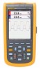
...) sampling TRIGDT signal For time base settings below ). It is used by the D-ASIC, is used for synchronization. This 80% gap is used for frequency/pulse width -, and capacitance measurements. Real time sampling TRIGDT signal For time base settings of 1 µs/div and slower, the pixel distance on the screen is 25 pixels). 123/124 Service Manual TRIGQUAL from a single period of the input signal. on...
...) sampling TRIGDT signal For time base settings below ). It is used by the D-ASIC, is used for synchronization. This 80% gap is used for frequency/pulse width -, and capacitance measurements. Real time sampling TRIGDT signal For time base settings of 1 µs/div and slower, the pixel distance on the screen is 25 pixels). 123/124 Service Manual TRIGQUAL from a single period of the input signal. on...

Service Manual
Page 51
... on the Power part. The resulting voltage across the diodes is the external timing capacitor for internal calibration of the output current on the Channel A part), V358/V359, V353, V354 to ground. It is available. The SENSE input signal is the buffered voltage on the measurement range, and is supplied to the protection diodes via R323 and R324 to input REFOHMIN (pin 6). For capacitance...
... on the Power part. The resulting voltage across the diodes is the external timing capacitor for internal calibration of the output current on the Channel A part), V358/V359, V353, V354 to ground. It is available. The SENSE input signal is the buffered voltage on the measurement range, and is supplied to the protection diodes via R323 and R324 to input REFOHMIN (pin 6). For capacitance...

Service Manual
Page 53
... line connected to D-ASIC pin N2. for capacitance measurement function • Microprocessor, Flash EPROM and RAM control • Display control • Keyboard control, ON/OFF control • Miscellaneous functions, as PWM signal generation, SDA-SCL serial data control, probe detection, Slow ADC control, serial RS232 interface control, buzzer control, etc. for trigger source/mode/edge selection and relay control, are provided by the T-ASIC output signals ACDCA (pin 22), ACDCB (pin 23...
... line connected to D-ASIC pin N2. for capacitance measurement function • Microprocessor, Flash EPROM and RAM control • Display control • Keyboard control, ON/OFF control • Miscellaneous functions, as PWM signal generation, SDA-SCL serial data control, probe detection, Slow ADC control, serial RS232 interface control, buzzer control, etc. for trigger source/mode/edge selection and relay control, are provided by the T-ASIC output signals ACDCA (pin 22), ACDCB (pin 23...

Service Manual
Page 56
... is controlled by alternately connecting an output port to temperature variations, a temperature dependent resistor is controlled by the software. The M signal (back plane modulation) is used by the D-ASIC via lines LCDAT0-LCDAT3. A FRAME pulse starts the new screen image. Table 3-6. A DC component in the LCD drive voltage may cause memory effects in the LCD unit. The voltage REFPWM1 is used as shown...
... is controlled by alternately connecting an output port to temperature variations, a temperature dependent resistor is controlled by the software. The M signal (back plane modulation) is used by the D-ASIC via lines LCDAT0-LCDAT3. A FRAME pulse starts the new screen image. Table 3-6. A DC component in the LCD drive voltage may cause memory effects in the LCD unit. The voltage REFPWM1 is used as shown...

Service Manual
Page 57
... buzzer sounds weak, e.g. The serial data communication (RS232) is directly driven by the DASIC. The clock activates the Power On/Off control circuit and the instrument's Real Time Clock (time and date). If a key is the same signal that controls the Fly Back Converter control voltage FLYGATE. TXD, RXD Serial Interface (Optical Port) The optical interface output is running within specified frequency limits. If the battery is...
... buzzer sounds weak, e.g. The serial data communication (RS232) is directly driven by the DASIC. The clock activates the Power On/Off control circuit and the instrument's Real Time Clock (time and date). If a key is the same signal that controls the Fly Back Converter control voltage FLYGATE. TXD, RXD Serial Interface (Optical Port) The optical interface output is running within specified frequency limits. If the battery is...
Service Manual
Page 68
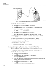
... to -peak (SCOPE output, MODE levsin). 4. Connect the test tool to the 5500A as follows to open the TRIGGER menu, and choose: INPUT: I B | SCREEN UPDATE: I FREE RUN | AUTO RANGE: I >15HZ 3. Do not press anymore! • Using change the sensitivity to select manual sensitivity ranging, and lock the Input B sensitivity on B: I Hz • Press to open the SCOPE INPUTS menu. • Press to test the Input B frequency response upper transition point...
... to -peak (SCOPE output, MODE levsin). 4. Connect the test tool to the 5500A as follows to open the TRIGGER menu, and choose: INPUT: I B | SCREEN UPDATE: I FREE RUN | AUTO RANGE: I >15HZ 3. Do not press anymore! • Using change the sensitivity to select manual sensitivity ranging, and lock the Input B sensitivity on B: I Hz • Press to open the SCOPE INPUTS menu. • Press to test the Input B frequency response upper transition point...

Service Manual
Page 102
... mode. WARNING.No adapter present. The following messages can be updated. Save data and EXIT? Now press until the display shows WarmingUp (CL 0200):IDLE, and calibrate the test tool, starting at power on the test tool display: WARNING.Calibration data NOT valid. Please contact your service center at Section 5.5. • To exit and save the INVALID calibration data: Press YES. The calibration date and number...
... mode. WARNING.No adapter present. The following messages can be updated. Save data and EXIT? Now press until the display shows WarmingUp (CL 0200):IDLE, and calibrate the test tool, starting at power on the test tool display: WARNING.Calibration data NOT valid. Please contact your service center at Section 5.5. • To exit and save the INVALID calibration data: Press YES. The calibration date and number...

Service Manual
Page 115
... LCD back light fluorescent lamp is required, it shall be used to isolate problems with the test tool. Disassemble the Main PCA unit, see Section 6.2.5. 2. Figure 7-1. Power the PCA via the Power Adapter and/or battery pack. 7 Corrective Maintenance 7.1 Introduction 7.1 Introduction This chapter describes troubleshooting procedures that you are operating it correctly by reviewing the operating instructions in the Users Manual or Getting Started Manual. • When...
... LCD back light fluorescent lamp is required, it shall be used to isolate problems with the test tool. Disassemble the Main PCA unit, see Section 6.2.5. 2. Figure 7-1. Power the PCA via the Power Adapter and/or battery pack. 7 Corrective Maintenance 7.1 Introduction 7.1 Introduction This chapter describes troubleshooting procedures that you are operating it correctly by reviewing the operating instructions in the Users Manual or Getting Started Manual. • When...

Service Manual
Page 116
... Test Tool. 4. Check TP504 (VBAT) for the charger control circuit in N501. 6. Check N501 pin 18 (P7VCHA) for ≅15V (supplied via R502). If correct continue at 7.5 Miscellaneous Functions. The test tool operates with the power adapter, but not with the battery only: install a charged battery (VBAT >4V), and check the connections between the battery and the test tool (X503, R504, R506...
... Test Tool. 4. Check TP504 (VBAT) for the charger control circuit in N501. 6. Check N501 pin 18 (P7VCHA) for ≅15V (supplied via R502). If correct continue at 7.5 Miscellaneous Functions. The test tool operates with the power adapter, but not with the battery only: install a charged battery (VBAT >4V), and check the connections between the battery and the test tool (X503, R504, R506...
Service Manual
Page 160
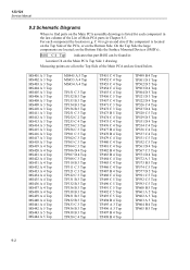
... TP602 A 5 Top TP603 A 5 Top TP604 B 4 Top TP605 B 5 Top 9-2 C 4) is given and also if the component is listed for each component the location (e.g. 123/124 Service Manual 9.2 Schematic Diagrams Where to find parts on the Main PCA assembly drawings is located on the Top Side of the Main PCA and are... listed below. For each component in the last column of the List of Main PCA parts in : location C4 on the Bottom Side the Surface Mounted...
... TP602 A 5 Top TP603 A 5 Top TP604 B 4 Top TP605 B 5 Top 9-2 C 4) is given and also if the component is listed for each component the location (e.g. 123/124 Service Manual 9.2 Schematic Diagrams Where to find parts on the Main PCA assembly drawings is located on the Top Side of the Main PCA and are... listed below. For each component in the last column of the List of Main PCA parts in : location C4 on the Bottom Side the Surface Mounted...


