
Operating Instructions
Page 4
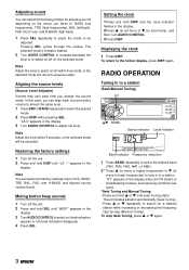
...this case, you change the source mode. Setting the clock 1 Press and hold i or k until the clock indicator flashes in stereo, and receiving conditions are good. *Seek Tuning and Manual Tuning • Press and hold DISP until seek Tuning starts. Displaying the clock 1 Press DISP. "ST" appears in the... display when an FM station is broadcasting in the display. 2 Press i (to set hour) or k (to select the desired mode. 2 Press DISP while pressing SEL. ...
...this case, you change the source mode. Setting the clock 1 Press and hold i or k until the clock indicator flashes in stereo, and receiving conditions are good. *Seek Tuning and Manual Tuning • Press and hold DISP until seek Tuning starts. Displaying the clock 1 Press DISP. "ST" appears in the... display when an FM station is broadcasting in the display. 2 Press i (to set hour) or k (to select the desired mode. 2 Press DISP while pressing SEL. ...
Operating Instructions
Page 6
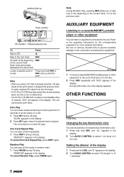
... start playing back, but this is not a malfunction. • If a CD-R or CD-RW with no data or incompatible data is already inserted, CD play . Setting the dimmer of all the tracks in the display. Note • When you find the point. "REPEAT1" appears in random order. 1 Press RNDM during CD...
... start playing back, but this is not a malfunction. • If a CD-R or CD-RW with no data or incompatible data is already inserted, CD play . Setting the dimmer of all the tracks in the display. Note • When you find the point. "REPEAT1" appears in random order. 1 Press RNDM during CD...
Service Manual
Page 28
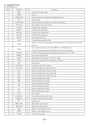
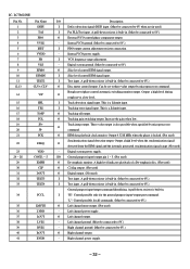
... for receiving from 13 CQCK O SQ OUT. "H"= MONO, "L"= ST FM reception. 14 SD/ST I System clock oscillator input. 2 TEST2 - LM- Normal set to "L". 39 CD ON O CD power switch output. - 28 - Not connected. 5 CD CLOCK IN I Initial setting diode matrix input. 31 VDD - IC DESCRIPTION IC, LC72358N-9A71 Pin No. Not connected. 35 FEM...
... for receiving from 13 CQCK O SQ OUT. "H"= MONO, "L"= ST FM reception. 14 SD/ST I System clock oscillator input. 2 TEST2 - LM- Normal set to "L". 39 CD ON O CD power switch output. - 28 - Not connected. 5 CD CLOCK IN I Initial setting diode matrix input. 31 VDD - IC DESCRIPTION IC, LC72358N-9A71 Pin No. Not connected. 35 FEM...
Service Manual
Page 31
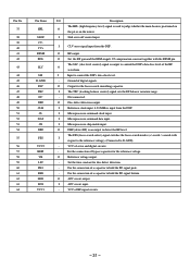
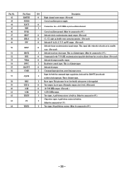
O RF output. O Disc defect detection output. VCC of bypass capacitor for the reference voltage. O APC circuit output. I Reference clock input. 4.23 MHz is input from the DSP. The SLC (slice level control) signal is an output to control the DSP's data ...NC DEF CLK CL DAT CE DRF FSS VCC2 REFI VR LF2 PH1 BH1 LDD LDS VCC1 I APC circuit input. - I Microprocessor command clock input. I The TBC (tracking balance control) signal sets the EF balance variation range. - I Microprocessor command data input. I Input to hold the RF signal peak. - I Sled servo off...
O RF output. O Disc defect detection output. VCC of bypass capacitor for the reference voltage. O APC circuit output. I Reference clock input. 4.23 MHz is input from the DSP. The SLC (slice level control) signal is an output to control the DSP's data ...NC DEF CLK CL DAT CE DRF FSS VCC2 REFI VR LF2 PH1 BH1 LDD LDS VCC1 I APC circuit input. - I Microprocessor command clock input. I The TBC (tracking balance control) signal sets the EF balance variation range. - I Microprocessor command data input. I Input to hold the RF signal peak. - I Sled servo off...
Service Manual
Page 32
... connection. - Left channel ground. (Must be connected to 0V.) General purpose input/output command identifying. IC, LC78622NE Pin No. This is built-in . (Must be set to 0V.) I Test input. A pull-down resistor is built-in used ) - Internal VCO ground. (Must be connected to three-value output by microprocessor O command. A pull...
... connection. - Left channel ground. (Must be connected to 0V.) General purpose input/output command identifying. IC, LC78622NE Pin No. This is built-in . (Must be set to 0V.) I Test input. A pull-down resistor is built-in used ) - Internal VCO ground. (Must be connected to three-value output by microprocessor O command. A pull...
Service Manual
Page 33
... a Schmitt input. I (Must be connected to 0V.) - 33 - This is a Schmitt input. (Must be set low briefly after power is Schmitt input. This pin must be connected to 0V.) O Subcode clock synchronization signal output. (Not used) O C1, C2, sigle an double error correction monitor. (Not used) O Subcode... the crystal oscillator. (Not used) O Subcode Q output standby output. O Connection for both the command input acquisition clock and the SQOUT pin subcode I readout clock input pin. This signal falls when the subcode are in . (Must be connected to 0 V.) O Output pin...
... a Schmitt input. I (Must be connected to 0V.) - 33 - This is a Schmitt input. (Must be set low briefly after power is Schmitt input. This pin must be connected to 0V.) O Subcode clock synchronization signal output. (Not used) O C1, C2, sigle an double error correction monitor. (Not used) O Subcode... the crystal oscillator. (Not used) O Subcode Q output standby output. O Connection for both the command input acquisition clock and the SQOUT pin subcode I readout clock input pin. This signal falls when the subcode are in . (Must be connected to 0 V.) O Output pin...
