Service Manual
Page 1
...include missing connectors. Replaced History Information and Front Cover pages. LCD DIGITAL COLOR TELEVISION 9-883-782-02 HISTORY INFORMATION FOR THE FOLLOWING MANUAL: SERVICE MANUAL MODEL NAME REMOTE COMMANDER KDL-52V4100 ☛ KDL-52V4100 KDL-52W4100 ☛ KDL-52W4100 RM-YD023 RM-YD023 RM-YD023 RM-YD023 EX1 ... Replaced pages 71, 73 and 75. Replaced page 83 Updated 4-2. Replaced pages 88-112. Updated D4Z, D5, and G5 schematics to include other destinations. Replaced page 84 Updated the Electrical Parts List to include BU Board part numbers for Mexico and Latin America...
...include missing connectors. Replaced History Information and Front Cover pages. LCD DIGITAL COLOR TELEVISION 9-883-782-02 HISTORY INFORMATION FOR THE FOLLOWING MANUAL: SERVICE MANUAL MODEL NAME REMOTE COMMANDER KDL-52V4100 ☛ KDL-52V4100 KDL-52W4100 ☛ KDL-52W4100 RM-YD023 RM-YD023 RM-YD023 RM-YD023 EX1 ... Replaced pages 71, 73 and 75. Replaced page 83 Updated 4-2. Replaced pages 88-112. Updated D4Z, D5, and G5 schematics to include other destinations. Replaced page 84 Updated the Electrical Parts List to include BU Board part numbers for Mexico and Latin America...

Service Manual
Page 3
... D4Z Board Schematic Diagram 71 D5 Board Schematic Diagram 73 G5 Board Schematic Diagram 75 H3E Board Schematic Diagram 78 H4 Board Schematic Diagram 80 3-5. Semiconductors 82 SECTION 4: EXPLODED VIEWS 83 4-1. Stand and Under Cover Removal 15 1-6. LCD Panel Removal 17 1-10.Balancer (ETC-Inverter MT) Board Removal 18 WIRE DRESSING 19 KDL-52V4100 Only 19 KDL-52W4100 Only...
... D4Z Board Schematic Diagram 71 D5 Board Schematic Diagram 73 G5 Board Schematic Diagram 75 H3E Board Schematic Diagram 78 H4 Board Schematic Diagram 80 3-5. Semiconductors 82 SECTION 4: EXPLODED VIEWS 83 4-1. Stand and Under Cover Removal 15 1-6. LCD Panel Removal 17 1-10.Balancer (ETC-Inverter MT) Board Removal 18 WIRE DRESSING 19 KDL-52V4100 Only 19 KDL-52W4100 Only...
Service Manual
Page 6
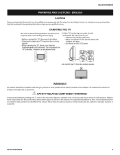
...fied by Sony. mark on the LCD panel. • When carrying the TV, place your hand as shown in this manual or in the operating instructions unless you are for use by placing your palm directly property and avoid causing serious injury. KDL-52V4100/52W4100 WARNINGS AND CAUTIONS...components are critical for safe operation. KDL-52V4100/52W4100 6 Do not subject the TV to protect your fingers in the groove above the • Carrying the large size TV requires two or more speaker grill area people. • put stress on the schematic diagrams, exploded views, and in...
...fied by Sony. mark on the LCD panel. • When carrying the TV, place your hand as shown in this manual or in the operating instructions unless you are for use by placing your palm directly property and avoid causing serious injury. KDL-52V4100/52W4100 WARNINGS AND CAUTIONS...components are critical for safe operation. KDL-52V4100/52W4100 6 Do not subject the TV to protect your fingers in the groove above the • Carrying the large size TV requires two or more speaker grill area people. • put stress on the schematic diagrams, exploded views, and in...
Service Manual
Page 8
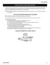
... shock, fire, or other hazard. When installing the LCD panel on the rear cover. KDL-52V4100/52W4100 SAFETY-RELATED COMPONENT WARNING There are critical components used in LCD color TVs that these critical parts be secured using a wrist band. do not press on the schematic diagrams and the electrical parts list. disconnect the AC adapter...
... shock, fire, or other hazard. When installing the LCD panel on the rear cover. KDL-52V4100/52W4100 SAFETY-RELATED COMPONENT WARNING There are critical components used in LCD color TVs that these critical parts be secured using a wrist band. do not press on the schematic diagrams and the electrical parts list. disconnect the AC adapter...
Service Manual
Page 55
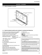
...electrolytics are critical for safety. symbol are in 50V unless otherwise specified. The symbol indicates a fast operating fuse and is as marked. KDL-52V4100/52W4100 55 Readings are in ohms. kΩ=1000Ω, MΩ=1000kΩ Indication of the same rating as follows: Pitch : 5mm Rating... ground : earth-chassis All variable and adjustable resistors have characteristic curve B, unless otherwise noted. PRINTED WIRING BOARDS AND SCHEMATIC DIAGRAMS INFORMATION All capacitors are taken with part number specified. Ne les remplacer que par une piece portant le...
...electrolytics are critical for safety. symbol are in 50V unless otherwise specified. The symbol indicates a fast operating fuse and is as marked. KDL-52V4100/52W4100 55 Readings are in ohms. kΩ=1000Ω, MΩ=1000kΩ Indication of the same rating as follows: Pitch : 5mm Rating... ground : earth-chassis All variable and adjustable resistors have characteristic curve B, unless otherwise noted. PRINTED WIRING BOARDS AND SCHEMATIC DIAGRAMS INFORMATION All capacitors are taken with part number specified. Ne les remplacer que par une piece portant le...

Service Manual
Page 58
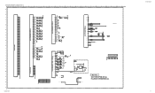
... M ComponentInput2 BL2 - VideoInput1 C - I /O A-1506-055-A BU-P1 KDL-52V4100/52W4100 58 R4 *J1101 O - SCHEMATICS AND SUPPORTING INFORMATION BU BOARD SCHEMATIC DIAGRAM (1 OF 12) 1 | 2 | 3 | 4 | 5 | 6 | 7 | 8 | 9 | 10 | 11 | 12 | 13 | 14 | 15 | 16 | 17 | 18 | 19 | 20 | 21 | 22 | 23 | 24 A - VideoInput3 E - K G1 - 3-4. J - H VideoInput2 - BL1 ComponentInput1 R1 L L1 - R3 N L2 - P KDL-52V4100/52W4100 VD1001 GND 4 4 2 2 6 3 3 1 1 VD1003 5 V1 9 10 7 8 V1_DET...
... M ComponentInput2 BL2 - VideoInput1 C - I /O A-1506-055-A BU-P1 KDL-52V4100/52W4100 58 R4 *J1101 O - SCHEMATICS AND SUPPORTING INFORMATION BU BOARD SCHEMATIC DIAGRAM (1 OF 12) 1 | 2 | 3 | 4 | 5 | 6 | 7 | 8 | 9 | 10 | 11 | 12 | 13 | 14 | 15 | 16 | 17 | 18 | 19 | 20 | 21 | 22 | 23 | 24 A - VideoInput3 E - K G1 - 3-4. J - H VideoInput2 - BL1 ComponentInput1 R1 L L1 - R3 N L2 - P KDL-52V4100/52W4100 VD1001 GND 4 4 2 2 6 3 3 1 1 VD1003 5 V1 9 10 7 8 V1_DET...

Service Manual
Page 60
...-A BU-P3 1 UVCC 2 XTRST 3 XRSTIN 4 XINIT 5 BREAK 6 ICD3 7 ICD2 8 ICD1 9 ICD0 10 ICS2 11 ICS1 12 ICS0 13 GND 14 ICLK CN3001 14P KDL-52V4100/52W4100 KDL-52V4100/52W4100 60 E - C - G - M - BU BOARD SCHEMATIC DIAGRAM (3 OF 12) 1 | 2 | 3 | 4 | 5 | 6 | 7 | 8 | 9 | 10 | 11 | 12 | 13 | 14 | 15 | 16 | 17 | 18 | 19 | 20 | 21 | 22 A - B - J - P C3006 0.1 16V 1005... A21/P55 60 A20/P54 59 A19/P53 58 A18/P52 57 A17/P51 56 A16/P50 55 VDDI 54 VSS 53 VDDE 52 A15 51 A14 50 A13 49 A12 48 A11 47 A10 46 A9 45 ICS2 ICS1 ICS0 R3038 DCC_LUT_SEL1 0 CHIP PANEL_SET_ON2 1005...
...-A BU-P3 1 UVCC 2 XTRST 3 XRSTIN 4 XINIT 5 BREAK 6 ICD3 7 ICD2 8 ICD1 9 ICD0 10 ICS2 11 ICS1 12 ICS0 13 GND 14 ICLK CN3001 14P KDL-52V4100/52W4100 KDL-52V4100/52W4100 60 E - C - G - M - BU BOARD SCHEMATIC DIAGRAM (3 OF 12) 1 | 2 | 3 | 4 | 5 | 6 | 7 | 8 | 9 | 10 | 11 | 12 | 13 | 14 | 15 | 16 | 17 | 18 | 19 | 20 | 21 | 22 A - B - J - P C3006 0.1 16V 1005... A21/P55 60 A20/P54 59 A19/P53 58 A18/P52 57 A17/P51 56 A16/P50 55 VDDI 54 VSS 53 VDDE 52 A15 51 A14 50 A13 49 A12 48 A11 47 A10 46 A9 45 ICS2 ICS1 ICS0 R3038 DCC_LUT_SEL1 0 CHIP PANEL_SET_ON2 1005...

Service Manual
Page 61
...RXE_CN RXE_CP RXE_N3 RXE_P3 RXE_N4 RXE_P4 from uCOM DIMMER R4818 0 CHIP 1005 DIMMER_DRV_OUT To G-brd BU 4/12 TRIDENT WX-2 KDL-52V4100/52W4100 RXE_P4 RXE_N4 RXE_P3 RXE_N3 RXE_CP RXE_CN RXE_P2 RXE_N2 RXE_P1 RXE_N1 RXE_P0 RXE_N0 RXO_P4 RXO_N4 RXO_P3 RXO_N3 RXO_CP RXO_CN RXO_P2 RXO_N2... GND 46 GND 47 POWER 48 POWER 49 POWER 50 POWER 51 POWER GND BLK CN4700 51P TO PANEL A-1506-055-A BU-P4 KDL-52V4100/52W4100 61 BU BOARD SCHEMATIC DIAGRAM (4 OF 12) 1 | 2 | 3 | 4 | 5 | 6 | 7 | 8 | 9 | 10 | 11 | 12 | 13 | 14 | 15 | 16 | 17 | 18 | 19 | 20 | 21 | 22 | 23 A ...
...RXE_CN RXE_CP RXE_N3 RXE_P3 RXE_N4 RXE_P4 from uCOM DIMMER R4818 0 CHIP 1005 DIMMER_DRV_OUT To G-brd BU 4/12 TRIDENT WX-2 KDL-52V4100/52W4100 RXE_P4 RXE_N4 RXE_P3 RXE_N3 RXE_CP RXE_CN RXE_P2 RXE_N2 RXE_P1 RXE_N1 RXE_P0 RXE_N0 RXO_P4 RXO_N4 RXO_P3 RXO_N3 RXO_CP RXO_CN RXO_P2 RXO_N2... GND 46 GND 47 POWER 48 POWER 49 POWER 50 POWER 51 POWER GND BLK CN4700 51P TO PANEL A-1506-055-A BU-P4 KDL-52V4100/52W4100 61 BU BOARD SCHEMATIC DIAGRAM (4 OF 12) 1 | 2 | 3 | 4 | 5 | 6 | 7 | 8 | 9 | 10 | 11 | 12 | 13 | 14 | 15 | 16 | 17 | 18 | 19 | 20 | 21 | 22 | 23 A ...

Service Manual
Page 64
N - BU BOARD SCHEMATIC DIAGRAM (7 OF 12) 1 | 2 | 3 | 4 | 5 | 6 | 7 | 8 | 9 | 10 | 11 | 12 | 13 | 14 | 15 | 16 | 17 | 18 | 19 | 20 | A - D - E - M - P REG12V F7005 1.6A 36V L7006 10uH 1.1A C7028 4.7 16V X7R 3216 ... 6.3V X6S 2012 C7165 10 6.3V X6S 2012 C7168 0.1 16V X7R 1005 C7184 220 16V GND BU 7/12 POWER SUPPLY A-1506-055-A BU-P7 21 | KDL-52V4100/52W4100 KDL-52V4100/52W4100 64 B - F - I - L - O - H - K - C - J - G -
N - BU BOARD SCHEMATIC DIAGRAM (7 OF 12) 1 | 2 | 3 | 4 | 5 | 6 | 7 | 8 | 9 | 10 | 11 | 12 | 13 | 14 | 15 | 16 | 17 | 18 | 19 | 20 | A - D - E - M - P REG12V F7005 1.6A 36V L7006 10uH 1.1A C7028 4.7 16V X7R 3216 ... 6.3V X6S 2012 C7165 10 6.3V X6S 2012 C7168 0.1 16V X7R 1005 C7184 220 16V GND BU 7/12 POWER SUPPLY A-1506-055-A BU-P7 21 | KDL-52V4100/52W4100 KDL-52V4100/52W4100 64 B - F - I - L - O - H - K - C - J - G -
Service Manual
Page 65
E - H - L - J - N - BU BOARD SCHEMATIC DIAGRAM (8 OF 12) 1 | 2 | 3 | 4 | 5 | 6 | 7 | 8 | 9 | 10 | 11 | 12 | 13 | 14 | 15 | 16 | 17 | 18 | 19 | 20 | 21 | 22 | 23 | A - ... 100 IRTXDA IRRXDA C14 CL7216 D14 CL7206 42 31 42 31 8642 7531 UART1_RXD UART1_TXD TO TV GPX_HSYNC_IN GPX_VSYNC_IN UART0_RXD UART0_TXD TO DIAG GPX_PCLK_IN RB7208 10k RB7210 10k SPI_CLK SPI_OUT SPI_DL_CS 24 13 ...ET7206 ET7207 GND BU 8/12 X245 GND/PWR/XTAL/ PLL/RESET/PERIPHERAL P A-1506-055-A BU-P8 KDL-52V4100/52W4100 KDL-52V4100/52W4100 65 M - G - D - I -
E - H - L - J - N - BU BOARD SCHEMATIC DIAGRAM (8 OF 12) 1 | 2 | 3 | 4 | 5 | 6 | 7 | 8 | 9 | 10 | 11 | 12 | 13 | 14 | 15 | 16 | 17 | 18 | 19 | 20 | 21 | 22 | 23 | A - ... 100 IRTXDA IRRXDA C14 CL7216 D14 CL7206 42 31 42 31 8642 7531 UART1_RXD UART1_TXD TO TV GPX_HSYNC_IN GPX_VSYNC_IN UART0_RXD UART0_TXD TO DIAG GPX_PCLK_IN RB7208 10k RB7210 10k SPI_CLK SPI_OUT SPI_DL_CS 24 13 ...ET7206 ET7207 GND BU 8/12 X245 GND/PWR/XTAL/ PLL/RESET/PERIPHERAL P A-1506-055-A BU-P8 KDL-52V4100/52W4100 KDL-52V4100/52W4100 65 M - G - D - I -

Service Manual
Page 66
C - J - L - H - M - O - G - E - N - BU BOARD SCHEMATIC DIAGRAM (9 OF 12) 1 | 2 | 3 | 4 | 5 | 6 | 7 | 8 | 9 | A - I - X245 NF INTERFACE X245 DDR2 INTERFACE (x16) D1.8V FB7401 0uH JL7409 C7406 0.1 16V 1005 GND DDR2 (x16) DQA_0 DQA_1 DQA_2 DQA_3 .../INT IC7000 215-0684001-00 AUDIO_MCLK FAD5_PAD D3.3V R7443 10k 1/16W CHIP BU 9/12 X245 DDR2/FLASH/NVM/FLEXBUS/STRAP A-1506-055-A BU-P9 KDL-52V4100/52W4100 KDL-52V4100/52W4100 66 D - F - B - K -
C - J - L - H - M - O - G - E - N - BU BOARD SCHEMATIC DIAGRAM (9 OF 12) 1 | 2 | 3 | 4 | 5 | 6 | 7 | 8 | 9 | A - I - X245 NF INTERFACE X245 DDR2 INTERFACE (x16) D1.8V FB7401 0uH JL7409 C7406 0.1 16V 1005 GND DDR2 (x16) DQA_0 DQA_1 DQA_2 DQA_3 .../INT IC7000 215-0684001-00 AUDIO_MCLK FAD5_PAD D3.3V R7443 10k 1/16W CHIP BU 9/12 X245 DDR2/FLASH/NVM/FLEXBUS/STRAP A-1506-055-A BU-P9 KDL-52V4100/52W4100 KDL-52V4100/52W4100 66 D - F - B - K -

Service Manual
Page 68
...A5V_TU IF_MONI A32V_MONI IF_AGC D_IF1 D_IF2 A5V_VIF AFT_OUT DET_OUT AGND ST_ID SAP_ID MODO F_MONO A9V_MPX R_OUT L_OUT A5V_DD GND GND SONY TUNER BTF-CA422T D3.3V CL7615 R7609 3.3k 1/16W CHIP C7649 4.7 10V X7R 2012 C7655 0.1 16V ... 1/16W CHIP 5% CL7620 R7677 100 1/16W CHIP R7682 220 1/16W CHIP 5% Q7605 2SA2122G0LS0 GND TV_M_MON_V BU 11/12 X245 FRONTEND/ADC/GPIOC/TUNER P KDL-52V4100/52W4100 A-1506-055-A BU-P11 KDL-52V4100/52W4100 68 I - N - B - H - J - BU BOARD SCHEMATIC DIAGRAM (11 OF 12) 1 | 2 | 3 | 4 | 5 | 6 | 7 | 8 | 9 | 10 | 11 | 12 | 13 | 14 | 15 | 16 ...
...A5V_TU IF_MONI A32V_MONI IF_AGC D_IF1 D_IF2 A5V_VIF AFT_OUT DET_OUT AGND ST_ID SAP_ID MODO F_MONO A9V_MPX R_OUT L_OUT A5V_DD GND GND SONY TUNER BTF-CA422T D3.3V CL7615 R7609 3.3k 1/16W CHIP C7649 4.7 10V X7R 2012 C7655 0.1 16V ... 1/16W CHIP 5% CL7620 R7677 100 1/16W CHIP R7682 220 1/16W CHIP 5% Q7605 2SA2122G0LS0 GND TV_M_MON_V BU 11/12 X245 FRONTEND/ADC/GPIOC/TUNER P KDL-52V4100/52W4100 A-1506-055-A BU-P11 KDL-52V4100/52W4100 68 I - N - B - H - J - BU BOARD SCHEMATIC DIAGRAM (11 OF 12) 1 | 2 | 3 | 4 | 5 | 6 | 7 | 8 | 9 | 10 | 11 | 12 | 13 | 14 | 15 | 16 ...

Service Manual
Page 69
....2 GND Y1 Y2 C7804 0.1 16V 1005 GND IC7000 215-0684001-00 D3.3V D2.5V D1.2V BU 12/12 X245 DVO OUTPUT (ITU656.GRAPHICS) P KDL-52V4100/52W4100 A-1506-055-A BU-P12 KDL-52V4100/52W4100 69 L - N - D - I - O - H - K - E - B - BU BOARD SCHEMATIC DIAGRAM (12 OF 12) 1 | 2 | 3 | 4 | 5 | 6 | 7 | 8 | 9 | 10 | 11 | 12 | 13 | 14 | 15 | 16 | 17 | 18 | 19 | 20 | 21...
....2 GND Y1 Y2 C7804 0.1 16V 1005 GND IC7000 215-0684001-00 D3.3V D2.5V D1.2V BU 12/12 X245 DVO OUTPUT (ITU656.GRAPHICS) P KDL-52V4100/52W4100 A-1506-055-A BU-P12 KDL-52V4100/52W4100 69 L - N - D - I - O - H - K - E - B - BU BOARD SCHEMATIC DIAGRAM (12 OF 12) 1 | 2 | 3 | 4 | 5 | 6 | 7 | 8 | 9 | 10 | 11 | 12 | 13 | 14 | 15 | 16 | 17 | 18 | 19 | 20 | 21...

Service Manual
Page 75
... UNREG_15V 4 UNREG_15V 3 STBY3.3V 2 AC_OFF_DET 1 POWER_ON CN6150 13P TO BU GND_1 1 REG12V 2 REG12V 3 REG12V_GND 4 REG12V_GND CN6100 4P TO TCON (KDL-52W4100 C6159 3300 25V R6158 47k 1/10W RN-CP MAIN FB 4 1 3 2 PH6100 PC123Y22FZW TMP R6150 680 1/10W RN-CP 5% R6151 1k 1/... X7R Q6402 RT1P14BC-TP-1 Q6403 RT1N14BC-TP-1 GND_1 C6407 1 25V X7R R6403 1k TMP D6401 MA113 PROT1 G5 POWER A-1511-323-A G5 KDL-52V4100/52W4100 KDL-52V4100/52W4100 75 ☛G5 BOARD SCHEMATIC DIAGRAM 1 | 2 | 3 | 4 | 5 | 6 | 7 | 8 | 9 | 10 | 11 | 12 | 13 | 14 | 15 | 16 | 17 | 18 | 19 | ...
... UNREG_15V 4 UNREG_15V 3 STBY3.3V 2 AC_OFF_DET 1 POWER_ON CN6150 13P TO BU GND_1 1 REG12V 2 REG12V 3 REG12V_GND 4 REG12V_GND CN6100 4P TO TCON (KDL-52W4100 C6159 3300 25V R6158 47k 1/10W RN-CP MAIN FB 4 1 3 2 PH6100 PC123Y22FZW TMP R6150 680 1/10W RN-CP 5% R6151 1k 1/... X7R Q6402 RT1P14BC-TP-1 Q6403 RT1N14BC-TP-1 GND_1 C6407 1 25V X7R R6403 1k TMP D6401 MA113 PROT1 G5 POWER A-1511-323-A G5 KDL-52V4100/52W4100 KDL-52V4100/52W4100 75 ☛G5 BOARD SCHEMATIC DIAGRAM 1 | 2 | 3 | 4 | 5 | 6 | 7 | 8 | 9 | 10 | 11 | 12 | 13 | 14 | 15 | 16 | 17 | 18 | 19 | ...

Service Manual
Page 78
B - H - E PICTURE OFF[RED&GREEN] TIMER[RED] - KDL-52V4100/52W4100 CL304 CL305 R305 1k 1/16W 0.5% Q305 UNR52A1G0LS0 D308 FR1105W STANDBY[RED] 654 7 GC2 GC1 NC IOUTGND VCC 123 *C302 0.1 .../RESERVE 4 STBY_LED 5 ON_TIMER 6 PWR/RESERVE 7 PICTURE_OFF 8 BL_IN 9 VD3.3V *CN301 9P TO BU BOARD CN3201 H3E LED/OPTICAL SENSOR A-1550-477-A H3E KDL-52V4100/52W4100 78 C - POWER[GREEN] F - I - H3E BOARD SCHEMATIC DIAGRAM 1 | 2 | 3 | 4 | 5 | 6 | 7 | 8 | 9 | 10 | 11 | 12 | 13 VYPY1105W D323 FR1105W D324 VYPY1105W D325 *IC301 *D302 A - G - CL301 R301 220 ...
B - H - E PICTURE OFF[RED&GREEN] TIMER[RED] - KDL-52V4100/52W4100 CL304 CL305 R305 1k 1/16W 0.5% Q305 UNR52A1G0LS0 D308 FR1105W STANDBY[RED] 654 7 GC2 GC1 NC IOUTGND VCC 123 *C302 0.1 .../RESERVE 4 STBY_LED 5 ON_TIMER 6 PWR/RESERVE 7 PICTURE_OFF 8 BL_IN 9 VD3.3V *CN301 9P TO BU BOARD CN3201 H3E LED/OPTICAL SENSOR A-1550-477-A H3E KDL-52V4100/52W4100 78 C - POWER[GREEN] F - I - H3E BOARD SCHEMATIC DIAGRAM 1 | 2 | 3 | 4 | 5 | 6 | 7 | 8 | 9 | 10 | 11 | 12 | 13 VYPY1105W D323 FR1105W D324 VYPY1105W D325 *IC301 *D302 A - G - CL301 R301 220 ...

Service Manual
Page 80
C 5% CHIP 1/16W 470 C14002 6.3V X6S R402 47 1/16W CHIP 5% - G KDL-52V4100/52W4100 KDL-52V4100/52W4100 80 H4 BOARD SCHEMATIC DIAGRAM 1 | 2 | 3 | 4 | 5 | 6 | 7 A - A-1494-139-A H4 F - R401 2012 CL403 1 CL401 2 CL402 3 SIRCS STBY3.3V GND *CN401 3P D 1005 X7R 50V 220p C401 - E H4 SIRCS - GND2 GND1 B IC401 OUT VCC -
C 5% CHIP 1/16W 470 C14002 6.3V X6S R402 47 1/16W CHIP 5% - G KDL-52V4100/52W4100 KDL-52V4100/52W4100 80 H4 BOARD SCHEMATIC DIAGRAM 1 | 2 | 3 | 4 | 5 | 6 | 7 A - A-1494-139-A H4 F - R401 2012 CL403 1 CL401 2 CL402 3 SIRCS STBY3.3V GND *CN401 3P D 1005 X7R 50V 220p C401 - E H4 SIRCS - GND2 GND1 B IC401 OUT VCC -

Service Manual
Page 114
SERVICE MANUAL EX1 CHASSIS In an effort to the Service Promotion Department at Service_Promotion@am.sony.com. To receive a complete set of this pdf file the tiled schematics are not attached to this manual please submit a request to reduce the size of the tiled schematics for this Service Manual.
SERVICE MANUAL EX1 CHASSIS In an effort to the Service Promotion Department at Service_Promotion@am.sony.com. To receive a complete set of this pdf file the tiled schematics are not attached to this manual please submit a request to reduce the size of the tiled schematics for this Service Manual.


