Service Manual
Page 1
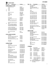
... 153-8654, Japan PIONEER ELECTRONICS SERVICE, INC. PIONEER ELECTRONIC (EUROPE) N.V. ZZM APR. 1998 Printed in Japan Box 1760, Long Beach, CA 90801-1760, U.S.A. RRV1943 ÷ Refer to the service manual RRV1889 for DV-505/KU. ADJUSTMENT 16 5. Haven 1087, Keetberglaan 1, 9120 Melsele, Belgium PIONEER ELECTRONICS ASIACENTRE PTE. CONTRAST OF MISCELLANEOUS PARTS ........ 2 2. P.O. DVD PLAYER DV-606D ORDER NO.
... 153-8654, Japan PIONEER ELECTRONICS SERVICE, INC. PIONEER ELECTRONIC (EUROPE) N.V. ZZM APR. 1998 Printed in Japan Box 1760, Long Beach, CA 90801-1760, U.S.A. RRV1943 ÷ Refer to the service manual RRV1889 for DV-505/KU. ADJUSTMENT 16 5. Haven 1087, Keetberglaan 1, 9120 Melsele, Belgium PIONEER ELECTRONICS ASIACENTRE PTE. CONTRAST OF MISCELLANEOUS PARTS ........ 2 2. P.O. DVD PLAYER DV-606D ORDER NO.
Service Manual
Page 2
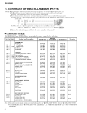
... 7 3 J 0.5 R50 RN2H R 5 0 K 1 1R0 RS1P 1 R 0 K Ex.2 When there are not in the service manual for the following examples. DV-606D/KU DV-606D/KC P5- 1 P5- 2 P6- 2 P6- 3 NSP ASSEMBLIES FLKY Assy FLKB Assy PWSB Assy DVDM Assy AVJB Assy VWM1789 VWG1873 VWG1879 VWS1326 VWV1572 VWM1794 VWG1878 VWG1939... on "7 EXPLOEDE VIEWS". SCHEMATIC DIAGRAM" and "3. indicate the pages and Nos. No. Mark Symbol and Description DV-505/KU Part No. DV-606D 1. Therefore, when replacing, be sure to use parts of the part. in our Master Spare Parts List. PCB CONNECTION DIAGRAM". 2
... 7 3 J 0.5 R50 RN2H R 5 0 K 1 1R0 RS1P 1 R 0 K Ex.2 When there are not in the service manual for the following examples. DV-606D/KU DV-606D/KC P5- 1 P5- 2 P6- 2 P6- 3 NSP ASSEMBLIES FLKY Assy FLKB Assy PWSB Assy DVDM Assy AVJB Assy VWM1789 VWG1873 VWG1879 VWS1326 VWV1572 VWM1794 VWG1878 VWG1939... on "7 EXPLOEDE VIEWS". SCHEMATIC DIAGRAM" and "3. indicate the pages and Nos. No. Mark Symbol and Description DV-505/KU Part No. DV-606D 1. Therefore, when replacing, be sure to use parts of the part. in our Master Spare Parts List. PCB CONNECTION DIAGRAM". 2
Service Manual
Page 4
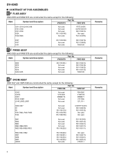
DV-606D CONTRAST OF PCB ASSEMBLIES FLKB ASSY VWG1878 and VWG1873 are constructed the same except for the following : Mark Symbol and Description Part No. VWS1326 VWS1327 IC602 IC6003 IC801 F9141,F9921 L9143,L9930,L9931 Not used VYW1559 MB86371A Not used Not used PDK026C VYW1546 MB86371 VTF1096.../10S432J RS1/10S622J RS1/10S103J RSG1030 DVDM ASSY VWS1327 and VWS1326 are constructed the same except for the following : Mark Symbol and Description Part No. VWG1873 VWG1878 Q101,Q104,Q106-Q108 D101-D108 R101-R108 R124 R126,R606 Not used Not used Not used RS1/10S0R0J Not used...
DV-606D CONTRAST OF PCB ASSEMBLIES FLKB ASSY VWG1878 and VWG1873 are constructed the same except for the following : Mark Symbol and Description Part No. VWS1326 VWS1327 IC602 IC6003 IC801 F9141,F9921 L9143,L9930,L9931 Not used VYW1559 MB86371A Not used Not used PDK026C VYW1546 MB86371 VTF1096.../10S432J RS1/10S622J RS1/10S103J RSG1030 DVDM ASSY VWS1327 and VWS1326 are constructed the same except for the following : Mark Symbol and Description Part No. VWG1873 VWG1878 Q101,Q104,Q106-Q108 D101-D108 R101-R108 R124 R126,R606 Not used Not used Not used RS1/10S0R0J Not used...
Service Manual
Page 5
...C654,C752,C855 C552,C863,C874 C704,C804,C915,C916 C556 C873 C207,C208,C307,C308 Part No. BA4560F CY2081SL-611 NJM4556AM NJM78M05FA NJM78M08FA PCM1716E PD0236AM TC4W53F TC74HCU04AF TC7S02F TC7SH02F TC7WU04F 2PB709A ...CCSQCH330J50 CCSQCH331J50 CCSQCH331J50 CCSQCH331J50 CCSQCH470J50 CCSQCH470J50 CEAL101M6R3 CEAT100M50 CEAT101M10 CEAT101M10 CEAT101M10 CEAT101M16 CEAT102M6R3 CEAT1R0M50 CEAT221M16 CEAT470M16 DV-606D Mark No. CEAT470M16 CEAT471M6R3 CEBA101M16 CFTYA104J50 CKSQYB103K50 CKSQYB104K25 CKSQYB105K10 CKSQYF103Z50 CKSQYF103Z50 CKSQYF103Z50 CKSQYF103Z50 CKSQYF103Z50 CKSQYF103Z50 CKSQYF103Z50...
...C654,C752,C855 C552,C863,C874 C704,C804,C915,C916 C556 C873 C207,C208,C307,C308 Part No. BA4560F CY2081SL-611 NJM4556AM NJM78M05FA NJM78M08FA PCM1716E PD0236AM TC4W53F TC74HCU04AF TC7S02F TC7SH02F TC7WU04F 2PB709A ...CCSQCH330J50 CCSQCH331J50 CCSQCH331J50 CCSQCH331J50 CCSQCH470J50 CCSQCH470J50 CEAL101M6R3 CEAT100M50 CEAT101M10 CEAT101M10 CEAT101M10 CEAT101M16 CEAT102M6R3 CEAT1R0M50 CEAT221M16 CEAT470M16 DV-606D Mark No. CEAT470M16 CEAT471M6R3 CEBA101M16 CFTYA104J50 CKSQYB103K50 CKSQYB104K25 CKSQYB105K10 CKSQYF103Z50 CKSQYF103Z50 CKSQYF103Z50 CKSQYF103Z50 CKSQYF103Z50 CKSQYF103Z50 CKSQYF103Z50...
Service Manual
Page 7
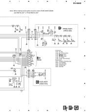
5 6 7 Note : When ordering service parts, be sure to refer to "EXPLODED VIEWS and PARTS LIST" or "PCB PARTS LIST". 8 DV-606D A 330 D202 SLP4118C51H 5.1CH MODE PWSB ASSY (VWG1939) D201 SLP9118C51H B AC1 AC2 H 2/3 CN105 FLKB ASSY S101 : FL OFF S102 : (OPEN/CLOSE) S103 : (REV) S104 : (FWD) S105 : (STOP) S106 : (PLAY/PAUSE) PWSB ASSY S201 : POWER (STANDBY/ON) S202 : 5.1CH MODE S203 : SUB WOOFER S204 : SURROUND S205 : CENTER C REMOTE RECEIVER UNIT G DILB ASSY (VWG1881) C112 0.1 R118 0 D G7 5 6 7 8
5 6 7 Note : When ordering service parts, be sure to refer to "EXPLODED VIEWS and PARTS LIST" or "PCB PARTS LIST". 8 DV-606D A 330 D202 SLP4118C51H 5.1CH MODE PWSB ASSY (VWG1939) D201 SLP9118C51H B AC1 AC2 H 2/3 CN105 FLKB ASSY S101 : FL OFF S102 : (OPEN/CLOSE) S103 : (REV) S104 : (FWD) S105 : (STOP) S106 : (PLAY/PAUSE) PWSB ASSY S201 : POWER (STANDBY/ON) S202 : 5.1CH MODE S203 : SUB WOOFER S204 : SURROUND S205 : CENTER C REMOTE RECEIVER UNIT G DILB ASSY (VWG1881) C112 0.1 R118 0 D G7 5 6 7 8
Service Manual
Page 14
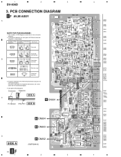
... Q753 Q901 IC231 Q931 IC231 Q701 Q801 Q702 Q802 Q804 Q805 Q807 Q808 Q761 IC651 Q762 Q853 Q852 IC601 Q771 Q772 4 The parts mounted on this PCB include all necessary parts for respective destinations, be sure to check with resistor B D G SD G S Field effect DGS transistor Resistor array 3-terminal regulator... information for several destinations. PCB CONNECTION DIAGRAM AVJB ASSY A NOTE FOR PCB DIAGRAMS : 1. Symbol In PCB Diagrams Symbol In Schematic Diagrams B C EB C E Part Name BCE Transistor BCE B C EB C E Transistor with the schematic diagram. 4. 1 2 3 DV-606D 3.
... Q753 Q901 IC231 Q931 IC231 Q701 Q801 Q702 Q802 Q804 Q805 Q807 Q808 Q761 IC651 Q762 Q853 Q852 IC601 Q771 Q772 4 The parts mounted on this PCB include all necessary parts for respective destinations, be sure to check with resistor B D G SD G S Field effect DGS transistor Resistor array 3-terminal regulator... information for several destinations. PCB CONNECTION DIAGRAM AVJB ASSY A NOTE FOR PCB DIAGRAMS : 1. Symbol In PCB Diagrams Symbol In Schematic Diagrams B C EB C E Part Name BCE Transistor BCE B C EB C E Transistor with the schematic diagram. 4. 1 2 3 DV-606D 3.