Service Manual
Page 12
4036-501 Acronyms ADF AGC AOC APS CCD CPU DADF DIMM E FTP GND HDD I/O JBIG JPEG KBS KL LDAP LVPS MFD MFP PDF PPM PWBA ROM S SE TIFF TTY UI VAC VDC Automatic Direction Finder Automatic Gain Control Abnormal Operating Condition Automatic Paper Size Charged Couple Device Central Processing Unit Duplex ...
4036-501 Acronyms ADF AGC AOC APS CCD CPU DADF DIMM E FTP GND HDD I/O JBIG JPEG KBS KL LDAP LVPS MFD MFP PDF PPM PWBA ROM S SE TIFF TTY UI VAC VDC Automatic Direction Finder Automatic Gain Control Abnormal Operating Condition Automatic Paper Size Charged Couple Device Central Processing Unit Duplex ...
Service Manual
Page 14
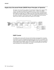
... sent to the control card. The voltage travels from the scanner cable into the scanner system board where it to the main power switch in ROM. Every electrical component within the DADF is necessary for the DADF to function. 4036-501 Duplex Auto Document Feeder (DADF) Power Principles of the processing...
... sent to the control card. The voltage travels from the scanner cable into the scanner system board where it to the main power switch in ROM. Every electrical component within the DADF is necessary for the DADF to function. 4036-501 Duplex Auto Document Feeder (DADF) Power Principles of the processing...
Service Manual
Page 34
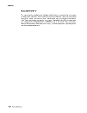
... the scanner send status information to the system card. switching on the results of the processing, the system card sends commands to function. Sensors in ROM.
... the scanner send status information to the system card. switching on the results of the processing, the system card sends commands to function. Sensors in ROM.

Service Manual
Page 151
4036-501 Signal name D0 D1 D2 D3 D4 D5 D6 D7 A0 MROMCS CRKITCS FLASHATC RD WR CRKTINT A1 A2 A3 A4 A5 A6 A7 Description CPU data bus 0 CPU data bus 1 CPU data bus 2 CPU data bus 3 CPU data bus 4 CPU data bus 5 CPU data bus 6 CPU data bus 7 CPU address bus 0 ROM chip selection Creation kit chip selection Flash ROM attachment signal Read signal from the CPU Write signal from the CPU Interruption signal to the creation kit CPU address bus 1 CPU address bus 2 CPU address bus 3 CPU address bus 4 CPU address bus 5 CPU address bus 6 CPU address bus 7 Connector Locations 5-25
4036-501 Signal name D0 D1 D2 D3 D4 D5 D6 D7 A0 MROMCS CRKITCS FLASHATC RD WR CRKTINT A1 A2 A3 A4 A5 A6 A7 Description CPU data bus 0 CPU data bus 1 CPU data bus 2 CPU data bus 3 CPU data bus 4 CPU data bus 5 CPU data bus 6 CPU data bus 7 CPU address bus 0 ROM chip selection Creation kit chip selection Flash ROM attachment signal Read signal from the CPU Write signal from the CPU Interruption signal to the creation kit CPU address bus 1 CPU address bus 2 CPU address bus 3 CPU address bus 4 CPU address bus 5 CPU address bus 6 CPU address bus 7 Connector Locations 5-25

Service Manual
Page 153
Description CPU address bus 8 CPU address bus 9 CPU address bus 10 CPU address bus 11 CPU address bus 12 CPU address bus 13 CPU address bus 14 CPU address bus 15 CPU address bus 16 CPU address bus 17 Creation kit status signal + Flash ROM switching signal between 8 bits and 16 bits Flash ROM busy signal Flash ROM reset signal Creation kit status signal Creation kit command signal + Creation kit command signal - 4036-501 Signal name A8 A9 A10 A11 A12 A13 A14 A15 A16 A17 CRKTSTS+ BYTE FROMBUSY RST CRKSTSCRKTCMD+ CRKTCMD- Connector Locations 5-27
Description CPU address bus 8 CPU address bus 9 CPU address bus 10 CPU address bus 11 CPU address bus 12 CPU address bus 13 CPU address bus 14 CPU address bus 15 CPU address bus 16 CPU address bus 17 Creation kit status signal + Flash ROM switching signal between 8 bits and 16 bits Flash ROM busy signal Flash ROM reset signal Creation kit status signal Creation kit command signal + Creation kit command signal - 4036-501 Signal name A8 A9 A10 A11 A12 A13 A14 A15 A16 A17 CRKTSTS+ BYTE FROMBUSY RST CRKSTSCRKTCMD+ CRKTCMD- Connector Locations 5-27