User Manual
Page 1
R P/I-P55T2P4 Pentium Motherboard USER'S MANUAL
R P/I-P55T2P4 Pentium Motherboard USER'S MANUAL
User Manual
Page 2
... system, or translated into any language in any form by the purchaser for backup purposes. ASUS may visit the ASUS home page at http://www.asus.com.tw/ or contact ASUS from the following page. © Copyright 1997 ASUSTeK COMPUTER INC. Manual updates are represented by the digit before and after the period of the... Corporation. • Sound Blaster AWE32 and SB16 are trademarks of Creative Technology Ltd. • Adobe and Acrobat are mentioned for identification purposes only. Product Name: ASUS P/I-P55T2P4 Manual Revision: 3.11 Release Date: May 1997 II...
... system, or translated into any language in any form by the purchaser for backup purposes. ASUS may visit the ASUS home page at http://www.asus.com.tw/ or contact ASUS from the following page. © Copyright 1997 ASUSTeK COMPUTER INC. Manual updates are represented by the digit before and after the period of the... Corporation. • Sound Blaster AWE32 and SB16 are trademarks of Creative Technology Ltd. • Adobe and Acrobat are mentioned for identification purposes only. Product Name: ASUS P/I-P55T2P4 Manual Revision: 3.11 Release Date: May 1997 II...
User Manual
Page 3
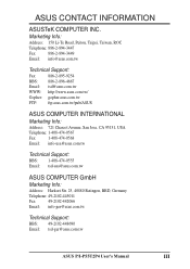
...-474-0555 Email: tsd-usa@asus.com.tw ASUS COMPUTER GmbH Marketing Info: Address: Harkort Str. 25, 40880 Ratingen, BRD, Germany Telephone: 49-2102-445011 Fax: 49-2102-442066 Email: info-ger@asus.com.tw Technical Support: BBS: 49-2102-448690 Email: tsd-ger@asus.com.tw ASUS P/I-P55T2P4 User's Manual III ASUS CONTACT INFORMATION ASUSTeK COMPUTER INC.
...-474-0555 Email: tsd-usa@asus.com.tw ASUS COMPUTER GmbH Marketing Info: Address: Harkort Str. 25, 40880 Ratingen, BRD, Germany Telephone: 49-2102-445011 Fax: 49-2102-442066 Email: info-ger@asus.com.tw Technical Support: BBS: 49-2102-448690 Email: tsd-ger@asus.com.tw ASUS P/I-P55T2P4 User's Manual III ASUS CONTACT INFORMATION ASUSTeK COMPUTER INC.
User Manual
Page 4
... Assigning IRQs for Expansion Cards 16 Assigning DMA Channels for this manual is organized 1 Item Checklist 1 II. BIOS Setup 29 Load Defaults 30 Standard CMOS Setup 30 IV ASUS P/I . System Memory (DRAM & SRAM 12 TAG SRAM Upgrade... of the ASUS Motherboard 2 Parts of the Motherboard 4 Installation Steps 6 1. INSTALLATION 4 Map of the ASUS Motherboard 3 III. External Connectors 19 Power Connection Procedures 25 IV. Jumpers 6 Jumper Settings 7 Cyrix CPU Identification 11 2. Central Processing Unit (CPU 15 4. CONTENTS I -P55T2P4 User's Manual INTRODUCTION 1 ...
... Assigning IRQs for Expansion Cards 16 Assigning DMA Channels for this manual is organized 1 Item Checklist 1 II. BIOS Setup 29 Load Defaults 30 Standard CMOS Setup 30 IV ASUS P/I . System Memory (DRAM & SRAM 12 TAG SRAM Upgrade... of the ASUS Motherboard 2 Parts of the Motherboard 4 Installation Steps 6 1. INSTALLATION 4 Map of the ASUS Motherboard 3 III. External Connectors 19 Power Connection Procedures 25 IV. Jumpers 6 Jumper Settings 7 Cyrix CPU Identification 11 2. Central Processing Unit (CPU 15 4. CONTENTS I -P55T2P4 User's Manual INTRODUCTION 1 ...
User Manual
Page 5
... (DMI 49 Introducing the ASUS DMI Configuration Utility 49 System Requirements 49 Using the ASUS DMI Configuration Utility 50 Notes 50 VI. ASUS I-A16C Audio Card 57 ASUS I -P55T2P4 User's Manual V ASUS PCI-SC200 SCSI Card 53 NCR SCSI BIOS and Drivers 53 The ASUS PCI-SC200 SCSI Interface Card... 54 Setting Up the ASUS PCI-SC200 54 Setting ...
... (DMI 49 Introducing the ASUS DMI Configuration Utility 49 System Requirements 49 Using the ASUS DMI Configuration Utility 50 Notes 50 VI. ASUS I-A16C Audio Card 57 ASUS I -P55T2P4 User's Manual V ASUS PCI-SC200 SCSI Card 53 NCR SCSI BIOS and Drivers 53 The ASUS PCI-SC200 SCSI Interface Card... 54 Setting Up the ASUS PCI-SC200 54 Setting ...
User Manual
Page 6
... Interference Regulations of the Canadian Department of the following two conditions: • This device may cause undesired operation. Canadian Department of the FCC Rules. VI ASUS P/I-P55T2P4 User's Manual This equipment has been tested and found to comply with FCC regulations. WARNING: The use of shielded cables for a Class B digital device, pursuant to...
... Interference Regulations of the Canadian Department of the following two conditions: • This device may cause undesired operation. Canadian Department of the FCC Rules. VI ASUS P/I-P55T2P4 User's Manual This equipment has been tested and found to comply with FCC regulations. WARNING: The use of shielded cables for a Class B digital device, pursuant to...
User Manual
Page 7
.../Win3.1x: Audio Software Manual (with mounting bracket Optional ASUS pipelined burst cache module ASUS P/I-P55T2P4 User's Manual 1 Features: Information and specifications concerning this manual is organized This manual is complete. BIOS Setup: BIOS software setup information. ASUS SCSI: Installation of the files • Technical Support Form This user's manual (Audio sections included with ASUS I-A16C audio bundle) Optional infrared...
.../Win3.1x: Audio Software Manual (with mounting bracket Optional ASUS pipelined burst cache module ASUS P/I-P55T2P4 User's Manual 1 Features: Information and specifications concerning this manual is organized This manual is complete. BIOS Setup: BIOS software setup information. ASUS SCSI: Installation of the files • Technical Support Form This user's manual (Audio sections included with ASUS I-A16C audio bundle) Optional infrared...
User Manual
Page 8
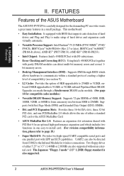
... a great many features in one PCI/MediaBus 2.0 which allows the use of either a standard PCI card or the ASUS MediaBus Card. • ASUS MediaBus Rev 2.0: Features an expansion slot extension shared with PCI Slot 4 for an optional high-performance expansion card which ...page 18.) • Super Multi-I -P55T2P4 User's Manual Two floppy drives of either 5.25" or 3.5" (1.44MB or 2.88MB) are made through BIOS which includes two functions in a small package. FEATURES Features of the ASUS Motherboard The ASUS P/I-P55T2P4 is also supported. 2 ASUS P/I /O: Provides two high-speed UART ...
... a great many features in one PCI/MediaBus 2.0 which allows the use of either a standard PCI card or the ASUS MediaBus Card. • ASUS MediaBus Rev 2.0: Features an expansion slot extension shared with PCI Slot 4 for an optional high-performance expansion card which ...page 18.) • Super Multi-I -P55T2P4 User's Manual Two floppy drives of either 5.25" or 3.5" (1.44MB or 2.88MB) are made through BIOS which includes two functions in a small package. FEATURES Features of the ASUS Motherboard The ASUS P/I-P55T2P4 is also supported. 2 ASUS P/I /O: Provides two high-speed UART ...
User Manual
Page 9
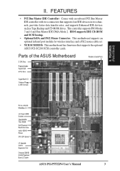
...8226; PCI Bus Master IDE Controller: Comes with an onboard PCI Bus Master IDE controller with two connectors that supports the optional ASUS PCI-SC200 SCSI controller cards. BIOS supports IDE CD-ROM and SCSI bootup. • Optional IrDA and PS/2 Mouse Connector...Bus Master IDE DMA Mode 2. II. Parts of Board) II. FEATURES (Parts of the ASUS Motherboard 3 ISA Slots Programmable Flash ROM 3 PCI Slots Parallel & Serial Ports Super Multi-I -P55T2P4 User's Manual 3 PCI 4 or ASUS MediaBus 2.0 (4) 72-pin SIMM Sockets Upgradeable TAG SRAM Self-Powered RealTime Clock Intel's 430HX ...
...8226; PCI Bus Master IDE Controller: Comes with an onboard PCI Bus Master IDE controller with two connectors that supports the optional ASUS PCI-SC200 SCSI controller cards. BIOS supports IDE CD-ROM and SCSI bootup. • Optional IrDA and PS/2 Mouse Connector...Bus Master IDE DMA Mode 2. II. Parts of Board) II. FEATURES (Parts of the ASUS Motherboard 3 ISA Slots Programmable Flash ROM 3 PCI Slots Parallel & Serial Ports Super Multi-I -P55T2P4 User's Manual 3 PCI 4 or ASUS MediaBus 2.0 (4) 72-pin SIMM Sockets Upgradeable TAG SRAM Self-Powered RealTime Clock Intel's 430HX ...
User Manual
Page 10
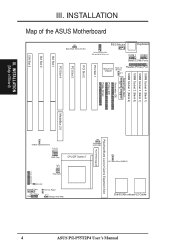
...) JP11 JP12 Case Connector Freq Ratio IDE LED Infrared Conn. CPU VCore JP20 12V Fan Power JP17 Voltage (STD/VRE) 256/512KB onboard L2 Cache 4 ASUS P/I /O (En/Dis) JP1 Parallel (Printer) Port PCI Slot 1 PCI Slot 2 PCI Slot 3 PCI Slot 4 ISA Slot 1 SIMM Socket 4 (Bank 1) SIMM ...Socket 3 (Bank 1) SIMM Socket 2 (Bank 0) SIMM Socket 1 (Bank 0) III. III. INSTALLATION (Map of the ASUS Motherboard ISA Slot 2 ISA Slot 3 JP2 Boot Block Write (Dis/En) PS/2 Mouse Keyboard Universal Serial Bus (Reserved for future use) COM 1 COM 2 Serial (COM...
...) JP11 JP12 Case Connector Freq Ratio IDE LED Infrared Conn. CPU VCore JP20 12V Fan Power JP17 Voltage (STD/VRE) 256/512KB onboard L2 Cache 4 ASUS P/I /O (En/Dis) JP1 Parallel (Printer) Port PCI Slot 1 PCI Slot 2 PCI Slot 3 PCI Slot 4 ISA Slot 1 SIMM Socket 4 (Bank 1) SIMM ...Socket 3 (Bank 1) SIMM Socket 2 (Bank 0) SIMM Socket 1 (Bank 0) III. III. INSTALLATION (Map of the ASUS Motherboard ISA Slot 2 ISA Slot 3 JP2 Boot Block Write (Dis/En) PS/2 Mouse Keyboard Universal Serial Bus (Reserved for future use) COM 1 COM 2 Serial (COM...
User Manual
Page 11
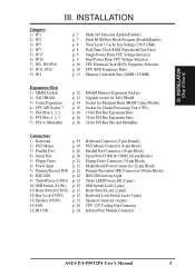
III. INSTALLATION Jumpers 1) JP1 2) JP2 3) JP5 4) JP7 5) JP17 6) JP20 7) JP8, JP9,JP10 8) JP11, JP12 9) JP4 p. 7 Multi-I -P55T2P4 User's Manual 5 IDE p. 22 8) IDE LED p. 22 9) Turbo/Power (CON1) p. 23 10) SMI Switch (CON1) p. 23 11) Reset Switch (CON1) p. 23 ...) SMI Switch Lead (2-pins) Reset Switch Lead (2-pins) Keyboard Lock Switch Lead (5-pins) Speaker Connector (4-pins) CPU 12V Cooling Fan Connector Infrared Port Module Connector ASUS P/I /O Selection (Enable/Disable) p. 7 Flash ROM Boot Block Program (Disable/Enable) p. 8 Total Level 2 Cache Size Setting (256/512KB) p. 8 Real ...
III. INSTALLATION Jumpers 1) JP1 2) JP2 3) JP5 4) JP7 5) JP17 6) JP20 7) JP8, JP9,JP10 8) JP11, JP12 9) JP4 p. 7 Multi-I -P55T2P4 User's Manual 5 IDE p. 22 8) IDE LED p. 22 9) Turbo/Power (CON1) p. 23 10) SMI Switch (CON1) p. 23 11) Reset Switch (CON1) p. 23 ...) SMI Switch Lead (2-pins) Reset Switch Lead (2-pins) Keyboard Lock Switch Lead (5-pins) Speaker Connector (4-pins) CPU 12V Cooling Fan Connector Infrared Port Module Connector ASUS P/I /O Selection (Enable/Disable) p. 7 Flash ROM Boot Block Program (Disable/Enable) p. 8 Total Level 2 Cache Size Setting (256/512KB) p. 8 Real ...
User Manual
Page 12
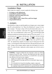
...are separated from other components against damage from yourself. See "Map of jumpers. For manufacturing simplicity, the jumpers may be sharing pins from the system. 6 ASUS P/I-P55T2P4 User's Manual Setup the BIOS Software 1. To connect the pins, simply place a plastic jumper cap over the two pins as [----], [1-2], [2-3] for loca- Place components on...as diagramed. Connect Ribbon Cables, Cabinet Wires, and Power Supply 6. A "1" is always on top or on the board. Use the diagrams in this manual instead of jumper caps to touch the IC chips, leads, or circuitry. 3.
...are separated from other components against damage from yourself. See "Map of jumpers. For manufacturing simplicity, the jumpers may be sharing pins from the system. 6 ASUS P/I-P55T2P4 User's Manual Setup the BIOS Software 1. To connect the pins, simply place a plastic jumper cap over the two pins as [----], [1-2], [2-3] for loca- Place components on...as diagramed. Connect Ribbon Cables, Cabinet Wires, and Power Supply 6. A "1" is always on top or on the board. Use the diagrams in this manual instead of jumper caps to touch the IC chips, leads, or circuitry. 3.
User Manual
Page 13
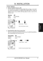
... once with the following jumper in order to allow programming in the Enabled position. Selections Enable Disable JP1 [1-2] (Default) [2-3] JP1 1 2 3 Enable (Default) JP1 1 2 3 Disabled Multi I -P55T2P4 User's Manual 7 Programming Disabled Enabled JP2 [1-2] (Default) [2-3] JP2 123 Disabled (Default) JP2 123 Enabled Boot Block Programming (Disable / Enable...
... once with the following jumper in order to allow programming in the Enabled position. Selections Enable Disable JP1 [1-2] (Default) [2-3] JP1 1 2 3 Enable (Default) JP1 1 2 3 Disabled Multi I -P55T2P4 User's Manual 7 Programming Disabled Enabled JP2 [1-2] (Default) [2-3] JP2 123 Disabled (Default) JP2 123 Enabled Boot Block Programming (Disable / Enable...
User Manual
Page 14
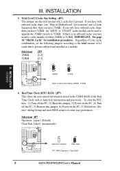
... you only have 256KB. Selections JP7 Operation [open] (Default) Clear Data [short] (momentarily) JP7 JP7 Operation (Default) Clear Data RTC RAM (Operation / Clear Data) 8 ASUS P/I-P55T2P4 User's Manual INSTALLATION (Jumpers) III. If you have onboard cache chips, then you may install a cache module of L2 cache that is present onboard and installed as...
... you only have 256KB. Selections JP7 Operation [open] (Default) Clear Data [short] (momentarily) JP7 JP7 Operation (Default) Clear Data RTC RAM (Operation / Clear Data) 8 ASUS P/I-P55T2P4 User's Manual INSTALLATION (Jumpers) III. If you have onboard cache chips, then you may install a cache module of L2 cache that is present onboard and installed as...
User Manual
Page 15
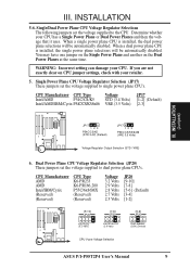
... 2.7 Volts 2.5 Volts JP20 [9-10] [7-8] [5-6] (Default) [3-4] [1-2] [9-10] JP20 K6-PR233 (3.2 Volts) [7-8] JP20 K6-PR166,200 (2.9 Volts) [5-6] JP20 P55C/6x86MX (2.8V) (Default) CPU Vcore Voltage Selection ASUS P/I-P55T2P4 User's Manual 9 Determine whether your retailer. 5. Single/Dual Power Plane CPU Voltage Regulator Selections The following jumpers set the voltage supplied to dual power plane CPU's. WARNING...
... 2.7 Volts 2.5 Volts JP20 [9-10] [7-8] [5-6] (Default) [3-4] [1-2] [9-10] JP20 K6-PR233 (3.2 Volts) [7-8] JP20 K6-PR166,200 (2.9 Volts) [5-6] JP20 P55C/6x86MX (2.8V) (Default) CPU Vcore Voltage Selection ASUS P/I-P55T2P4 User's Manual 9 Determine whether your retailer. 5. Single/Dual Power Plane CPU Voltage Regulator Selections The following jumpers set the voltage supplied to dual power plane CPU's. WARNING...
User Manual
Page 16
... clock generator what frequency to send to BUS Frequency Ratio (JP11, JP12) These jumpers set together with the Cyrix PR166+ installed on this motherboard. 10 ASUS P/I-P55T2P4 User's Manual JP8 JP9 JP10 JP8 JP9 JP10 JP8 JP9 JP10 JP8 JP9 JP10 JP8 JP9 JP10 1 1 1 1 2 2 2 2 3 3 3 3 50MHz 55MHz 60MHz 66MHz CPU External Clock (BUS) Frequency...
... clock generator what frequency to send to BUS Frequency Ratio (JP11, JP12) These jumpers set together with the Cyrix PR166+ installed on this motherboard. 10 ASUS P/I-P55T2P4 User's Manual JP8 JP9 JP10 JP8 JP9 JP10 JP8 JP9 JP10 JP8 JP9 JP10 JP8 JP9 JP10 1 1 1 1 2 2 2 2 3 3 3 3 50MHz 55MHz 60MHz 66MHz CPU External Clock (BUS) Frequency...
User Manual
Page 17
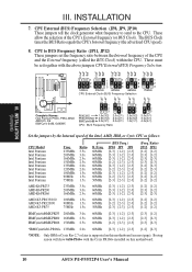
... Identification The only Cyrix CPU that you need to install a TAG SRAM upgrade or use a cache module with an extended TAG SRAM (such as 256KB ASUS CM1 Rev 3.0 with 2 TAG SRAM's) but must be Revision 2.7 or later. See "Map of pipelined burst SRAM chips, this jumper must be set this motherboard...) 512MB (BSRAM Only) JP4 [1-2] (Default) [2-3] JP4 123 64MB Cacheable (Default) Burst SRAM or MCache JP4 123 512MB Cacheable Burst SRAM Only Cacheable Size (64MB/512MB) ASUS P/I-P55T2P4 User's Manual 11
... Identification The only Cyrix CPU that you need to install a TAG SRAM upgrade or use a cache module with an extended TAG SRAM (such as 256KB ASUS CM1 Rev 3.0 with 2 TAG SRAM's) but must be Revision 2.7 or later. See "Map of pipelined burst SRAM chips, this jumper must be set this motherboard...) 512MB (BSRAM Only) JP4 [1-2] (Default) [2-3] JP4 123 64MB Cacheable (Default) Burst SRAM or MCache JP4 123 512MB Cacheable Burst SRAM Only Cacheable Size (64MB/512MB) ASUS P/I-P55T2P4 User's Manual 11
User Manual
Page 18
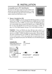
... module that is 15ns or faster. You must have an extended tag, do not install another TAG SRAM into the TAG SRAM Upgrade Socket. 12 ASUS P/I-P55T2P4 User's Manual III. Notch Indention Insert one 16K8 or 32K8 SRAM chip as shown by "Memory Cacheable Size" jumper. The DRAM can be unstable. TAG SRAM...
... module that is 15ns or faster. You must have an extended tag, do not install another TAG SRAM into the TAG SRAM Upgrade Socket. 12 ASUS P/I-P55T2P4 User's Manual III. Notch Indention Insert one 16K8 or 32K8 SRAM chip as shown by "Memory Cacheable Size" jumper. The DRAM can be unstable. TAG SRAM...
User Manual
Page 19
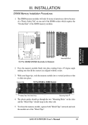
... Procedures: 1. Press the memory module firmly into place. The SIMM memory modules will only fit in SIMM Socket Safety Tab (This Side Only) Mounting Hole 4. ASUS P/I-P55T2P4 User's Manual 13 III.
... Procedures: 1. Press the memory module firmly into place. The SIMM memory modules will only fit in SIMM Socket Safety Tab (This Side Only) Mounting Hole 4. ASUS P/I-P55T2P4 User's Manual 13 III.
User Manual
Page 20
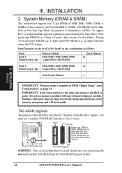
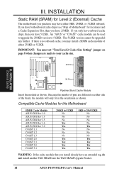
If you only have onboard cache chips, then you have 256KB. Compatible Cache Modules for this Motherboard SIMM Cache Module ASUS CM1 Rev 1.0 ASUS CM1 Rev 1.3 ASUS CM4 Rev 1.5 ASUS CM1 Rev 1.6 ASUS CM1 Rev 3.0 COAST 1.1 COAST 1.2 COAST 1.3 COAST 2.0 COAST 2.1 COAST 3.0 COAST 3.1 256KB to 512KB No No No ...Cache Expansion Slot, then you may have an extended tag, do not install another TAG SRAM into the TAG SRAM Upgrade Socket. 14 ASUS P/I-P55T2P4 User's Manual The 512KB version cannot be used to upgrade the 256KB version to 512KB. IMPORTANT: You must set "Total Level 2 Cache Size ...
If you only have onboard cache chips, then you have 256KB. Compatible Cache Modules for this Motherboard SIMM Cache Module ASUS CM1 Rev 1.0 ASUS CM1 Rev 1.3 ASUS CM4 Rev 1.5 ASUS CM1 Rev 1.6 ASUS CM1 Rev 3.0 COAST 1.1 COAST 1.2 COAST 1.3 COAST 2.0 COAST 2.1 COAST 3.0 COAST 3.1 256KB to 512KB No No No ...Cache Expansion Slot, then you may have an extended tag, do not install another TAG SRAM into the TAG SRAM Upgrade Socket. 14 ASUS P/I-P55T2P4 User's Manual The 512KB version cannot be used to upgrade the 256KB version to 512KB. IMPORTANT: You must set "Total Level 2 Cache Size ...


