Technical Reference
Page 15
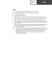
... 2-4 list the page sizes and dimensions of the physical page and the printable area in the following tables, see page 1-1 for information on the preceding diagram for your printer supports. 2-3 PCL Legend: A Portrait physical page width and landscape physical page length B Portrait physical page length and landscape physical page width C Portrait...
... 2-4 list the page sizes and dimensions of the physical page and the printable area in the following tables, see page 1-1 for information on the preceding diagram for your printer supports. 2-3 PCL Legend: A Portrait physical page width and landscape physical page length B Portrait physical page length and landscape physical page width C Portrait...
Technical Reference
Page 318
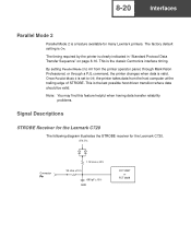
... this feature helpful when having data transfer reliability problems. Signal Descriptions STROBE Receiver for the Lexmark C720 The following diagram illustrates the STROBE receiver for many Lexmark printers. The timing required by the printer is a feature available for the Lexmark C720. +5V, 5% Connector Pin 1.1K ohm ±10% 33 ohm ±10% 690 pF...
... this feature helpful when having data transfer reliability problems. Signal Descriptions STROBE Receiver for the Lexmark C720 The following diagram illustrates the STROBE receiver for many Lexmark printers. The timing required by the printer is a feature available for the Lexmark C720. +5V, 5% Connector Pin 1.1K ohm ±10% 33 ohm ±10% 690 pF...
Technical Reference
Page 319
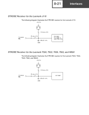
8-21 Interfaces STROBE Receiver for the Lexmark J110 The following diagram illustrates the STROBE receiver for the Lexmark J110. +5V, 5% Connector Pin 1.1K ohm ±10% 33 ohm ±10% 690 pF ±10% GND FCT 2827, FCT 2828, or ASIC PIN (J110) STROBE Receiver for the Lexmark T520, T522, T620, T622, and W820 The following diagram illustrates the STROBE receiver for the Lexmark T520, T522, T620, T622, and W820. +5V, 5% Connector Pin 1.1K ohm ±10% 33 ohm ±10% 620 pF ±10% GND FCT 2827
8-21 Interfaces STROBE Receiver for the Lexmark J110 The following diagram illustrates the STROBE receiver for the Lexmark J110. +5V, 5% Connector Pin 1.1K ohm ±10% 33 ohm ±10% 690 pF ±10% GND FCT 2827, FCT 2828, or ASIC PIN (J110) STROBE Receiver for the Lexmark T520, T522, T620, T622, and W820 The following diagram illustrates the STROBE receiver for the Lexmark T520, T522, T620, T622, and W820. +5V, 5% Connector Pin 1.1K ohm ±10% 33 ohm ±10% 620 pF ±10% GND FCT 2827
Technical Reference
Page 320
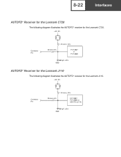
8-22 Interfaces AUTOFD* Receiver for the Lexmark C720 The following diagram illustrates the AUTOFD* receiver for the Lexmark C720. +5V, 5% Connector Pin 1.1K ohm ±10% 39 ohm ±5% FCT 2827 or FCT 2828 690 pF ±10% GND AUTOFD* Receiver for the Lexmark J110 The following diagram illustrates the AUTOFD* receiver for the Lexmark J110. +5V, 5% Connector Pin 1.1K ohm ±10% 39 ohm ±5% FCT 2827, FCT 2828, or ASIC Pin (J110) 690 pF ±10% GND
8-22 Interfaces AUTOFD* Receiver for the Lexmark C720 The following diagram illustrates the AUTOFD* receiver for the Lexmark C720. +5V, 5% Connector Pin 1.1K ohm ±10% 39 ohm ±5% FCT 2827 or FCT 2828 690 pF ±10% GND AUTOFD* Receiver for the Lexmark J110 The following diagram illustrates the AUTOFD* receiver for the Lexmark J110. +5V, 5% Connector Pin 1.1K ohm ±10% 39 ohm ±5% FCT 2827, FCT 2828, or ASIC Pin (J110) 690 pF ±10% GND
Technical Reference
Page 321
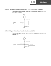
8-23 Interfaces AUTOFD* Receiver for the Lexmark T520, T522, T620, T622, and W820 The following diagram illustrates the AUTOFD* receiver for the Lexmark T520, T522, T620, T622, and W820. +5V, 5% Connector Pin 1.1K ohm ±10% 39 ohm ±5% FCT 2827 620 pF ±10% GND DATA 1-8 Signal Driver/Receivers for the Lexmark C720 The following diagram illustrates each of the DATA 1-8 signal driver/receivers for the Lexmark C720. +5V, 5% Connector Pin 2.2K ohm ±10% 33 ohm ±5% FCT 2245 220 pF ±20% GND
8-23 Interfaces AUTOFD* Receiver for the Lexmark T520, T522, T620, T622, and W820 The following diagram illustrates the AUTOFD* receiver for the Lexmark T520, T522, T620, T622, and W820. +5V, 5% Connector Pin 1.1K ohm ±10% 39 ohm ±5% FCT 2827 620 pF ±10% GND DATA 1-8 Signal Driver/Receivers for the Lexmark C720 The following diagram illustrates each of the DATA 1-8 signal driver/receivers for the Lexmark C720. +5V, 5% Connector Pin 2.2K ohm ±10% 33 ohm ±5% FCT 2245 220 pF ±20% GND
Technical Reference
Page 322
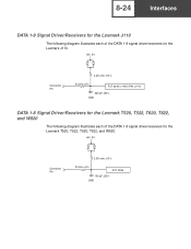
8-24 Interfaces DATA 1-8 Signal Driver/Receivers for the Lexmark J110 The following diagram illustrates each of the DATA 1-8 signal driver/receivers for the Lexmark J110. +5V, 5% Connector Pin 2.2K ohm ±10% 33 ohm ±5% FCT 2245 or ASIC PIN (J110) 220 pF ±20% GND DATA 1-8 Signal Driver/Receivers for the Lexmark T520, T522, T620, T622, and W820 The following diagram illustrates each of the DATA 1-8 signal driver/receivers for the Lexmark T520, T522, T620, T622, and W820. +5V, 5% Connector Pin 2.2K ohm ±10% 33 ohm ±5% FCT 2245 150 pF ±20% GND
8-24 Interfaces DATA 1-8 Signal Driver/Receivers for the Lexmark J110 The following diagram illustrates each of the DATA 1-8 signal driver/receivers for the Lexmark J110. +5V, 5% Connector Pin 2.2K ohm ±10% 33 ohm ±5% FCT 2245 or ASIC PIN (J110) 220 pF ±20% GND DATA 1-8 Signal Driver/Receivers for the Lexmark T520, T522, T620, T622, and W820 The following diagram illustrates each of the DATA 1-8 signal driver/receivers for the Lexmark T520, T522, T620, T622, and W820. +5V, 5% Connector Pin 2.2K ohm ±10% 33 ohm ±5% FCT 2245 150 pF ±20% GND
Technical Reference
Page 323
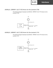
8-25 Interfaces ACKNLG*, ERROR*, SLCT, PE Drivers for the Lexmark C720 The following diagram illustrates the ACKNLG*, ERROR*, SLCT, PE drivers for the Lexmark C720. +5V FCT 2827 or FCT 2828 2.2K ohm ±10% 39 ohm ±5% 220 pF ±20% Connector Pin GND ACKNLG*, ERROR*, SLCT, PE Drivers for the Lexmark J110 The following diagram illustrates the ACKNLG*, ERROR*, SLCT, PE drivers for the Lexmark J110. +5V 2.2K ohm ±10% FCT 2827, FCT 2828, or ASIC (J110) 39 ohm ±5% 220 pF ±20% Connector Pin GND
8-25 Interfaces ACKNLG*, ERROR*, SLCT, PE Drivers for the Lexmark C720 The following diagram illustrates the ACKNLG*, ERROR*, SLCT, PE drivers for the Lexmark C720. +5V FCT 2827 or FCT 2828 2.2K ohm ±10% 39 ohm ±5% 220 pF ±20% Connector Pin GND ACKNLG*, ERROR*, SLCT, PE Drivers for the Lexmark J110 The following diagram illustrates the ACKNLG*, ERROR*, SLCT, PE drivers for the Lexmark J110. +5V 2.2K ohm ±10% FCT 2827, FCT 2828, or ASIC (J110) 39 ohm ±5% 220 pF ±20% Connector Pin GND
Technical Reference
Page 324
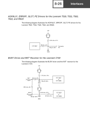
8-26 Interfaces ACKNLG*, ERROR*, SLCT, PE Drivers for the Lexmark T520, T522, T620, T622, and W820 The following diagram illustrates the ACKNLG*, ERROR*, SLCT, PE drivers for the Lexmark T520, T522, T620, T622, and W820. +5V 2.2K ohm ±10% FCT 2827 39 ohm ±5% 150 pF ±20% Connector Pin GND... BUSY Driver and INIT* Receiver for the Lexmark C720 The following diagram illustrates the BUSY driver and the INIT* ...
8-26 Interfaces ACKNLG*, ERROR*, SLCT, PE Drivers for the Lexmark T520, T522, T620, T622, and W820 The following diagram illustrates the ACKNLG*, ERROR*, SLCT, PE drivers for the Lexmark T520, T522, T620, T622, and W820. +5V 2.2K ohm ±10% FCT 2827 39 ohm ±5% 150 pF ±20% Connector Pin GND... BUSY Driver and INIT* Receiver for the Lexmark C720 The following diagram illustrates the BUSY driver and the INIT* ...

Technical Reference
Page 325
8-27 Interfaces BUSY Driver and INIT* Receiver for the Lexmark J110 The following diagram illustrates the BUSY driver and the INIT* receiver for the Lexmark J110. +5V 1.1K ohm ±10% INIT* 39 ohm ±5% (input) 1722 pF ±20% GND +5V 50K ohm ±5% FCT 2827, FCT 2828, or ASCI (J110) BUSY 2.2K ohm ±10% (output) 220 pF ±20% GND 39 ohm ±5% FCT 2827, FCT 2828, or ASCI (J110)
8-27 Interfaces BUSY Driver and INIT* Receiver for the Lexmark J110 The following diagram illustrates the BUSY driver and the INIT* receiver for the Lexmark J110. +5V 1.1K ohm ±10% INIT* 39 ohm ±5% (input) 1722 pF ±20% GND +5V 50K ohm ±5% FCT 2827, FCT 2828, or ASCI (J110) BUSY 2.2K ohm ±10% (output) 220 pF ±20% GND 39 ohm ±5% FCT 2827, FCT 2828, or ASCI (J110)

Technical Reference
Page 326
8-28 Interfaces BUSY Driver and INIT* Receiver for the Lexmark T520, T522, T620, T622, and W820 The following diagram illustrates the BUSY driver and the INIT* receiver for the Lexmark T520, T522, T620, T622, and W820. +5V 1.1K ohm ±10% INIT* 39 ohm ±5% (input) 1650 pF ±20% GND +5V 50K ohm ±5% FCT 2827 BUSY 2.2K ohm ±10% (output) 150 pF ±20% GND 39 ohm ±5% FCT 2827
8-28 Interfaces BUSY Driver and INIT* Receiver for the Lexmark T520, T522, T620, T622, and W820 The following diagram illustrates the BUSY driver and the INIT* receiver for the Lexmark T520, T522, T620, T622, and W820. +5V 1.1K ohm ±10% INIT* 39 ohm ±5% (input) 1650 pF ±20% GND +5V 50K ohm ±5% FCT 2827 BUSY 2.2K ohm ±10% (output) 150 pF ±20% GND 39 ohm ±5% FCT 2827
Technical Reference
Page 327
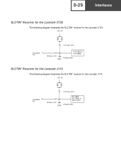
8-29 Interfaces SLCTIN* Receiver for the Lexmark C720 The following diagram illustrates the SLCTIN* receiver for the Lexmark C720. +5V, 5% Connector Pin 1.1K ohm ±10% 39 ohm ±10% GND FCT 2827 or FCT 2828 1720 pF ±20% SLCTIN* Receiver for the Lexmark J110 The following diagram illustrates the SLCTIN* receiver for the Lexmark J110. +5V, 5% Connector Pin 1.1K ohm ±10% 39 ohm ±10% GND FCT 2827, FCT 2828, or ASIC (J110) 1720 pF ±20%
8-29 Interfaces SLCTIN* Receiver for the Lexmark C720 The following diagram illustrates the SLCTIN* receiver for the Lexmark C720. +5V, 5% Connector Pin 1.1K ohm ±10% 39 ohm ±10% GND FCT 2827 or FCT 2828 1720 pF ±20% SLCTIN* Receiver for the Lexmark J110 The following diagram illustrates the SLCTIN* receiver for the Lexmark J110. +5V, 5% Connector Pin 1.1K ohm ±10% 39 ohm ±10% GND FCT 2827, FCT 2828, or ASIC (J110) 1720 pF ±20%
Technical Reference
Page 328
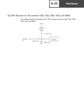
8-30 Interfaces SLCTIN* Receiver for the Lexmark T520, T522, T620, T622, and W820 The following diagram illustrates the SLCTIN* receiver for the Lexmark T520, T522, T620, T622, and W820. +5V, 5% Connector Pin 1.1K ohm ±10% 39 ohm ±10% GND FCT 2827 1650 pF ±20%
8-30 Interfaces SLCTIN* Receiver for the Lexmark T520, T522, T620, T622, and W820 The following diagram illustrates the SLCTIN* receiver for the Lexmark T520, T522, T620, T622, and W820. +5V, 5% Connector Pin 1.1K ohm ±10% 39 ohm ±10% GND FCT 2827 1650 pF ±20%
Technical Reference
Page 336
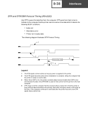
... pace the data flow from high to low to indicate to the computer that the printer cannot receive more data when it detects the following diagram illustrates DTR Protocol Timing. 1 2 3 Receive Data Valid 4 Legend: 1 The RTS signal is driven active as long as power is supplied to the printer. 2 The DTR...
... pace the data flow from high to low to indicate to the computer that the printer cannot receive more data when it detects the following diagram illustrates DTR Protocol Timing. 1 2 3 Receive Data Valid 4 Legend: 1 The RTS signal is driven active as long as power is supplied to the printer. 2 The DTR...
Technical Reference
Page 337
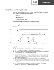
... on the setting of Honor DSR.) 4 After you select this data flow control protocol, the printer sends an XOFF signal when it detects the following diagram illustrates XON/XOFF Protocol Timing. 1 RTS DTR 2 DSR 3 Receive Data Valid XMT RXD XON 4 XOFF XON 5 6 Legend: 1 The RTS signal is driven active as long...
... on the setting of Honor DSR.) 4 After you select this data flow control protocol, the printer sends an XOFF signal when it detects the following diagram illustrates XON/XOFF Protocol Timing. 1 RTS DTR 2 DSR 3 Receive Data Valid XMT RXD XON 4 XOFF XON 5 6 Legend: 1 The RTS signal is driven active as long...