Design Guide
Page 4
...60 2.14 AC'97 ...2-61 2.14.1 AC'97 Signal Quality Requirements 2-63 2.14.2 AC'97 Motherboard Implementation 2-63 2.15 USB ...2-65 2.16 ISA (82380AB 2-66 2.16.1 ICH GPIO connected to 82380AB...3-4 3.2.1 Initial Timing Analysis 3-5 3.2.2 Determine General Topology, Layout, and Routing Desired ...........3-8 3.2.3 Pre-Layout Simulation 3-8 3.2.4 Place and Route Board 3-10 3.2.5 Post-Layout Simulation 3-13 3.2.6 Validation 3-14 3.3 Theory...3-15 3.3.1 AGTL 3-15 3.3.2 Timing Requirements 3-16 3.3.3 Cross-talk Theory... 3-20 3.4.4 Clock Routing 3-23 iv Intel® 820 Chipset Design Guide
...60 2.14 AC'97 ...2-61 2.14.1 AC'97 Signal Quality Requirements 2-63 2.14.2 AC'97 Motherboard Implementation 2-63 2.15 USB ...2-65 2.16 ISA (82380AB 2-66 2.16.1 ICH GPIO connected to 82380AB...3-4 3.2.1 Initial Timing Analysis 3-5 3.2.2 Determine General Topology, Layout, and Routing Desired ...........3-8 3.2.3 Pre-Layout Simulation 3-8 3.2.4 Place and Route Board 3-10 3.2.5 Post-Layout Simulation 3-13 3.2.6 Validation 3-14 3.3 Theory...3-15 3.3.1 AGTL 3-15 3.3.2 Timing Requirements 3-16 3.3.3 Cross-talk Theory... 3-20 3.4.4 Clock Routing 3-23 iv Intel® 820 Chipset Design Guide

Design Guide
Page 5
... 5-1 5.3.2 PCB Materials 5-2 5.3.3 Design Process 5-2 5.3.4 Test Coupon Design Guidelines 5-3 5.3.5 Recommended Stackup 5-3 5.3.6 Inner Layer Routing 5-3 5.3.7 Impedance Calculation Tools 5-4 5.3.8 Testing Board Impedance 5-4 5.3.9 Board Impedance/Stackup Summary 5-5 6 System Design Considerations 6-1 6.1 Power Delivery 6-1 6.1.1 Terminology and Definitions 6-1 6.1.2 Intel® 820 Chipset Customer Reference Board Power Delivery ......6-2 6.1.3 64/72Mbit RDRAM Excessive Power Consumption 6-5 6.2 Power Plane Splits 6-7 6.3 Thermal Design Power 6-7 6.4 Glue Chip...
... 5-1 5.3.2 PCB Materials 5-2 5.3.3 Design Process 5-2 5.3.4 Test Coupon Design Guidelines 5-3 5.3.5 Recommended Stackup 5-3 5.3.6 Inner Layer Routing 5-3 5.3.7 Impedance Calculation Tools 5-4 5.3.8 Testing Board Impedance 5-4 5.3.9 Board Impedance/Stackup Summary 5-5 6 System Design Considerations 6-1 6.1 Power Delivery 6-1 6.1.1 Terminology and Definitions 6-1 6.1.2 Intel® 820 Chipset Customer Reference Board Power Delivery ......6-2 6.1.3 64/72Mbit RDRAM Excessive Power Consumption 6-5 6.2 Power Plane Splits 6-7 6.3 Thermal Design Power 6-7 6.4 Glue Chip...
Design Guide
Page 13
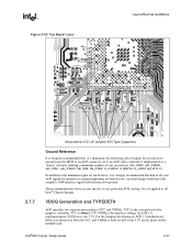
... designs, the core schematics for each chipset component remains the same for most Intel® 820 chipset platforms. The appendices provides a set of schematics for the board design is also provided. The motherboard functional units are discussed. This chapter provides motherboard clocking guidelines (e.g., clock architecture, routing, capacitor sites, clock power decoupling, and clock skew...
... designs, the core schematics for each chipset component remains the same for most Intel® 820 chipset platforms. The appendices provides a set of schematics for the board design is also provided. The motherboard functional units are discussed. This chapter provides motherboard clocking guidelines (e.g., clock architecture, routing, capacitor sites, clock power decoupling, and clock skew...

Design Guide
Page 22
... Audio Modem Codec (AMC) (Figure 1-4c), or separate audio and modem codecs can be connected to the ICH. This reduces configuration errors. Intel® 820 chipset's integrated digital link allows two external codecs to be connected to the ICH (Figure 1-4d). Microphone input and left and ...the platform migrates away from ISA. Modem implementation for cost-effective, high-quality, integrated audio on -board and the modem codec can be implemented with an appropriate modem codec. 1-10 Intel®820 Chipset Design Guide The digital link in the ICH is also supported with the use ...
... Audio Modem Codec (AMC) (Figure 1-4c), or separate audio and modem codecs can be connected to the ICH. This reduces configuration errors. Intel® 820 chipset's integrated digital link allows two external codecs to be connected to the ICH (Figure 1-4d). Microphone input and left and ...the platform migrates away from ISA. Modem implementation for cost-effective, high-quality, integrated audio on -board and the modem codec can be implemented with an appropriate modem codec. 1-10 Intel®820 Chipset Design Guide The digital link in the ICH is also supported with the use ...

Design Guide
Page 39
... splits. The return current will require the Vterm island to be on the top layer. In a 4 layer board, this will flow through the Vterm capacitors into the ground island and under the RSL traces. Intel®820 Chipset Design Guide 2-13 Layout/Routing Guidelines 2.6.2.3 Direct Rambus* Ground Plane Reference All RSL signals...
... splits. The return current will require the Vterm island to be on the top layer. In a 4 layer board, this will flow through the Vterm capacitors into the ground island and under the RSL traces. Intel®820 Chipset Design Guide 2-13 Layout/Routing Guidelines 2.6.2.3 Direct Rambus* Ground Plane Reference All RSL signals...

Design Guide
Page 47
...: the trace length on the board. • Nominal RSL Length: the length to allow for this package mismatch. The Nominal RSL Length is an arbitrary length (within the limits of RIMM connector, the length mismatch between the pad (on EITHER layer. Layout/Routing Guidelines Figure 2-22. Intel®820 Chipset Design Guide...
...: the trace length on the board. • Nominal RSL Length: the length to allow for this package mismatch. The Nominal RSL Length is an arbitrary length (within the limits of RIMM connector, the length mismatch between the pad (on EITHER layer. Layout/Routing Guidelines Figure 2-22. Intel®820 Chipset Design Guide...

Design Guide
Page 48
..., L2 -> Package Dimensions L3, L4 -> Board Trace Length L1 MCH Package MCH Die Ball L3 L2 L4 L1 + L3 = Nominal RSL Length ±10 mils L2 + L4 = Nominal RSL Length ±10 mils R R I I M M M M C C o o n n n n e e c c t t o o V r r t e r m NOTE: Refer to Chapter 4, "Clocking" for more information on Via Compensation. 2-22 Intel®820 Chipset Design Guide The...
..., L2 -> Package Dimensions L3, L4 -> Board Trace Length L1 MCH Package MCH Die Ball L3 L2 L4 L1 + L3 = Nominal RSL Length ±10 mils L2 + L4 = Nominal RSL Length ±10 mils R R I I M M M M C C o o n n n n e e c c t t o o V r r t e r m NOTE: Refer to Chapter 4, "Clocking" for more information on Via Compensation. 2-22 Intel®820 Chipset Design Guide The...

Design Guide
Page 61
...group should be as close to the pin on the same layer. When matching trace length for all signals within 0.1"). These guidelines apply to board stackups with 5 mil spacing when breaking out of the MCH to zero as possible. Layout/Routing Guidelines 2.7.4 This pair should be separated from... other signals by at least 20 mils (1:4). All AGP Interfaces The 2X/4X Timing Domain Signals can be routed with 10% impedance tolerance Intel®820 Chipset Design Guide 2-35 The strobe pair must be length matched to insure added margin. All signals in a signal group should...
...group should be as close to the pin on the same layer. When matching trace length for all signals within 0.1"). These guidelines apply to board stackups with 5 mil spacing when breaking out of the MCH to zero as possible. Layout/Routing Guidelines 2.7.4 This pair should be separated from... other signals by at least 20 mils (1:4). All AGP Interfaces The 2X/4X Timing Domain Signals can be routed with 10% impedance tolerance Intel®820 Chipset Design Guide 2-35 The strobe pair must be length matched to insure added margin. All signals in a signal group should...
Design Guide
Page 62
...is required per 10 vias. On a typical four layer PCB design the signals transition from one side of the board to replace thorough system validation on the motherboard, add-in the AGP Design Guide, Revision 1.0 (Section 1.5.3.3). Layout/Routing Guidelines 2.7.5 AGP Clock Routing The ...focus of clock skew (the motherboard designer shall determine how the 0.9 ns is to another. Recommendations Decoupling • For VDDQ decoupling, a minimum of space between the board and the synthesizer). This 1 ns includes skew and jitter which originates on Intel® 820 chipset based products...
...is required per 10 vias. On a typical four layer PCB design the signals transition from one side of the board to replace thorough system validation on the motherboard, add-in the AGP Design Guide, Revision 1.0 (Section 1.5.3.3). Layout/Routing Guidelines 2.7.5 AGP Clock Routing The ...focus of clock skew (the motherboard designer shall determine how the 0.9 ns is to another. Recommendations Decoupling • For VDDQ decoupling, a minimum of space between the board and the synthesizer). This 1 ns includes skew and jitter which originates on Intel® 820 chipset based products...
Design Guide
Page 63
... Chipset Design Guide 2-37 In AGP 1.0 implementations VDDQ was also 3.3V. For the designer developing an AGP 1.0 motherboard, there is no distinction between VCC and VDDQ as a "down" solution) utilizing a minimum number of all Intel® Chipset designs. VCC is the core power for the graphics controller. In addition to ground depending... Signal Layer Layout/Routing Guidelines 2.7.7 Must add six 0.01 uF ceramic 603 Type Capacitors Ground Reference It is strongly recommended that half of vias on board layout. Figure 2-30.
... Chipset Design Guide 2-37 In AGP 1.0 implementations VDDQ was also 3.3V. For the designer developing an AGP 1.0 motherboard, there is no distinction between VCC and VDDQ as a "down" solution) utilizing a minimum number of all Intel® Chipset designs. VCC is the core power for the graphics controller. In addition to ground depending... Signal Layer Layout/Routing Guidelines 2.7.7 Must add six 0.01 uF ceramic 603 Type Capacitors Ground Reference It is strongly recommended that half of vias on board layout. Figure 2-30.

Design Guide
Page 71
It can be used by the ICH to adjust buffer characteristics to specific board characteristics. Locally generated Hub Interface Reference Dividers 1.8V 1.8V 2.8.4 300Ω 300Ω HUBREF MCH 300Ω HubRef2.vsd 0.1uF 300Ω HUBREF ICH 0.1uF ...
It can be used by the ICH to adjust buffer characteristics to specific board characteristics. Locally generated Hub Interface Reference Dividers 1.8V 1.8V 2.8.4 300Ω 300Ω HUBREF MCH 300Ω HubRef2.vsd 0.1uF 300Ω HUBREF ICH 0.1uF ...

Design Guide
Page 72
...Figure 2-36. An example topology is valid for 133 MHz and 100 MHz 2-way processor/Intel® 820 chipset designs. The 82820 MCH should be placed on the base board. Intel® Pentium® III Processor Dual Processor Configuration Processor Processor L1 L2 L3 L(1,2,3): Z0 ...= 60Ω ± 15% MCH Table 2-12. Figure 2-37. Intel® Pentium® III Processor Uni-Processor Configuration MCH ...
...Figure 2-36. An example topology is valid for 133 MHz and 100 MHz 2-way processor/Intel® 820 chipset designs. The 82820 MCH should be placed on the base board. Intel® Pentium® III Processor Dual Processor Configuration Processor Processor L1 L2 L3 L(1,2,3): Z0 ...= 60Ω ± 15% MCH Table 2-12. Figure 2-37. Intel® Pentium® III Processor Uni-Processor Configuration MCH ...

Design Guide
Page 73
...ability and damage could occur to the SC242 connector. This keying is asymmetric, and requires 0.159" mounting holes. In a 4 layer board, this section. The most notable interface requirement to as the S.E.C.C.2 (Single Edge Contact Cartidge 2) Grounding Retention Mechanism (GRM). This ... the GRM asymmetric. The ground reference must be on the motherboard. Ground Plane Reference (Four Layer Motherboard) Required SC242 GND Plane 2.10 MCH 4laym pwr plane vsd S.E.C.C. 2 Grounding Retention Mechanism (GRM) Intel is the addition of grounding pads around two of the Retention...
...ability and damage could occur to the SC242 connector. This keying is asymmetric, and requires 0.159" mounting holes. In a 4 layer board, this section. The most notable interface requirement to as the S.E.C.C.2 (Single Edge Contact Cartidge 2) Grounding Retention Mechanism (GRM). This ... the GRM asymmetric. The ground reference must be on the motherboard. Ground Plane Reference (Four Layer Motherboard) Required SC242 GND Plane 2.10 MCH 4laym pwr plane vsd S.E.C.C. 2 Grounding Retention Mechanism (GRM) Intel is the addition of grounding pads around two of the Retention...

Design Guide
Page 74
... Dash lines represent control line for connector key features when placed on the top layer of the board, and possibly short out traces immediately beneath the solder mask, resulting in board failure. Retention mechanism must stay within Cross-Hatch area. 3. Drawing not to scale Figure 2-40...is a high risk that the metal clip that grounds to the motherboard will be plated and grounded with a minimum of eight VIAS. NOTES: 1. copper). 2-48 Intel®820 Chipset Design Guide Layout/Routing Guidelines Motherboard Interfaces Figure 2-39 shows the Hole Locations and Keepout Zones For ...
... Dash lines represent control line for connector key features when placed on the top layer of the board, and possibly short out traces immediately beneath the solder mask, resulting in board failure. Retention mechanism must stay within Cross-Hatch area. 3. Drawing not to scale Figure 2-40...is a high risk that the metal clip that grounds to the motherboard will be plated and grounded with a minimum of eight VIAS. NOTES: 1. copper). 2-48 Intel®820 Chipset Design Guide Layout/Routing Guidelines Motherboard Interfaces Figure 2-39 shows the Hole Locations and Keepout Zones For ...

Design Guide
Page 77
... CPU0. Connect to MCH HL10 pin Connect to GND. Tie to 2nd processor via 8.2 KΩ series resistor. Connect to simulate based on -board VR or VRM. Some of direct connection to simulate based on simulation results. Optional override (jumpers, ASIC, etc.) could be dual-ended or single...Table 2-13. If used . CPU0 and CPU1 should have internal pull-ups. Implement in same manner as CPU0. Intel®820 Chipset Design Guide 2-51 This checklist supports Intel® Pentium® II processors at the clock driver then route to CK133 SEL133/100# pin. May also connect ...
... CPU0. Connect to MCH HL10 pin Connect to GND. Tie to 2nd processor via 8.2 KΩ series resistor. Connect to simulate based on -board VR or VRM. Some of direct connection to simulate based on simulation results. Optional override (jumpers, ASIC, etc.) could be dual-ended or single...Table 2-13. If used . CPU0 and CPU1 should have internal pull-ups. Implement in same manner as CPU0. Intel®820 Chipset Design Guide 2-51 This checklist supports Intel® Pentium® II processors at the clock driver then route to CK133 SEL133/100# pin. May also connect ...

Design Guide
Page 79
... CPU #2 BREQ0# BREQ1# on -board logic must be connected to BREQ0 should be held for two clocks after the arbitration ID strapping is complete. The timing requirement of HA7# strapping is very similar to the CPURESET trace with a very short stub. Intel®820 Chipset Design Guide 2-53 Layout... connected to the BREQ0 AGTL trace with a very short stub. The value of RSTIN#. Additionally, the series current limiting resistor on -board logic tri-state BREQ0# after the deassertion of the BREQ connections in the previous section. Refer to the latest version of the on...
... CPU #2 BREQ0# BREQ1# on -board logic must be connected to BREQ0 should be held for two clocks after the arbitration ID strapping is complete. The timing requirement of HA7# strapping is very similar to the CPURESET trace with a very short stub. Intel®820 Chipset Design Guide 2-53 Layout... connected to the BREQ0 AGTL trace with a very short stub. The value of RSTIN#. Additionally, the series current limiting resistor on -board logic tri-state BREQ0# after the deassertion of the BREQ connections in the previous section. Refer to the latest version of the on...

Design Guide
Page 80
...production, do not add this circuit, since the overall system performance will work under the worst case condition. Also, Intel does not guarantee the above layout recommendation will be degraded. HA7# Strapping Option Example Circuit (For Debug Purposes Only... 4 2 D /PRE Q 5 3 CLK /Q 6 /CLR 1 74F74 4.7 KΩ jumper R2 4.7 KΩ HA7 2N3904 CPUCLK In-Target Probe (ITP) It is recommended that prototype boards implement the ITP connector. Layout/Routing Guidelines The recommendation for the debug situation that requires to set the IOQ depth equal to pull-up resistors...
...production, do not add this circuit, since the overall system performance will work under the worst case condition. Also, Intel does not guarantee the above layout recommendation will be degraded. HA7# Strapping Option Example Circuit (For Debug Purposes Only... 4 2 D /PRE Q 5 3 CLK /Q 6 /CLR 1 74F74 4.7 KΩ jumper R2 4.7 KΩ HA7 2N3904 CPUCLK In-Target Probe (ITP) It is recommended that prototype boards implement the ITP connector. Layout/Routing Guidelines The recommendation for the debug situation that requires to set the IOQ depth equal to pull-up resistors...
Design Guide
Page 81
...contained in separate groups to isolate AGTL+ signals from signals that have larger voltage swings, such as 5V PCI. • Select a board stack-up that can create a large undershoot, followed by more than the data lines and their corresponding control lines. Guidelines for VTT... 1 Processor Power Distribution Guidelines." • Place resistor divider pairs for the following general rules will minimize the impact of the design. Intel®820 Chipset Design Guide 2-55 Be sure to include decoupling capacitors. This can be simulated for VREF generation at least 0.025". ...
...contained in separate groups to isolate AGTL+ signals from signals that have larger voltage swings, such as 5V PCI. • Select a board stack-up that can create a large undershoot, followed by more than the data lines and their corresponding control lines. Guidelines for VTT... 1 Processor Power Distribution Guidelines." • Place resistor divider pairs for the following general rules will minimize the impact of the design. Intel®820 Chipset Design Guide 2-55 Be sure to include decoupling capacitors. This can be simulated for VREF generation at least 0.025". ...

Design Guide
Page 89
...link. The ICH has weak pulldowns/pullups that could be no connected (e.g., with the specified load of 50pF. 2.14.2 AC'97 Motherboard Implementation The following design considerations are no codecs present. These recommendations do not represent the only implementation or a complete checklist, but ...provides recommendations based on the link. On the Intel® 820 chipset platform, the ICH supports Wake on -board codec can be disabled, both SDIN pins must be implemented in the design. This will keep it implies...
...link. The ICH has weak pulldowns/pullups that could be no connected (e.g., with the specified load of 50pF. 2.14.2 AC'97 Motherboard Implementation The following design considerations are no codecs present. These recommendations do not represent the only implementation or a complete checklist, but ...provides recommendations based on the link. On the Intel® 820 chipset platform, the ICH supports Wake on -board codec can be disabled, both SDIN pins must be implemented in the design. This will keep it implies...

Design Guide
Page 95
...000 uAh / 3 uA = 56,666 h = 6.4 years The voltage of the battery can be obtained when the RTC voltage is an example of the board). • The oscillator VCC should be clean; To do this, the diodes are rated by storage capacity. around ¼ inch is sufficient. • ...connected to the RTC when available, which can be calculated by dividing the capacity by the average current required. Intel®820 Chipset Design Guide 2-69 Figure 2-57 is in a desktop system to provide continuous power to the ICH via an isolation schottky diode circuit. use a filter, such as...
...000 uAh / 3 uA = 56,666 h = 6.4 years The voltage of the battery can be obtained when the RTC voltage is an example of the board). • The oscillator VCC should be clean; To do this, the diodes are rated by storage capacity. around ¼ inch is sufficient. • ...connected to the RTC when available, which can be calculated by dividing the capacity by the average current required. Intel®820 Chipset Design Guide 2-69 Figure 2-57 is in a desktop system to provide continuous power to the ICH via an isolation schottky diode circuit. use a filter, such as...


