Design Guide
Page 4
...2.14 AC'97 ...2-61 2.14.1 AC'97 Signal Quality Requirements 2-63 2.14.2 AC'97 Motherboard Implementation 2-63 2.15 USB ...2-65 2.16 ISA (82380AB 2-66 2.16.1 ICH GPIO connected to 82380AB 2-66 2.16...3-4 3.2.1 Initial Timing Analysis 3-5 3.2.2 Determine General Topology, Layout, and Routing Desired ...........3-8 3.2.3 Pre-Layout Simulation 3-8 3.2.4 Place and Route Board 3-10 3.2.5 Post-Layout Simulation 3-13 3.2.6 Validation 3-14 3.3 Theory...3-15 3.3.1 AGTL 3-15 3.3.2 Timing Requirements 3-16 3.3.3 Cross-talk ... 3-20 3.4.4 Clock Routing 3-23 iv Intel® 820 Chipset Design Guide
...2.14 AC'97 ...2-61 2.14.1 AC'97 Signal Quality Requirements 2-63 2.14.2 AC'97 Motherboard Implementation 2-63 2.15 USB ...2-65 2.16 ISA (82380AB 2-66 2.16.1 ICH GPIO connected to 82380AB 2-66 2.16...3-4 3.2.1 Initial Timing Analysis 3-5 3.2.2 Determine General Topology, Layout, and Routing Desired ...........3-8 3.2.3 Pre-Layout Simulation 3-8 3.2.4 Place and Route Board 3-10 3.2.5 Post-Layout Simulation 3-13 3.2.6 Validation 3-14 3.3 Theory...3-15 3.3.1 AGTL 3-15 3.3.2 Timing Requirements 3-16 3.3.3 Cross-talk ... 3-20 3.4.4 Clock Routing 3-23 iv Intel® 820 Chipset Design Guide

Design Guide
Page 7
...22 One Layer with Multiple Reference Planes 3-22 Overdrive Region and VREF Guardband 3-25 Rising Edge Flight Time Measurement 3-25 Intel® 820 Chipset Platform Clock Distribution 4-2 Intel® 820 Chipset Clock Routing Guidelines 4-4 CK133 to DRCG Routing Diagram 4-6 MCH to DRCG Routing Diagram 4-7 Direct ... Secondary IDE Connector 2-61 Tee Topology AC'97 Trace Length Requirements 2-62 Daisy-Chain Topology AC'97 Trace Length Requirements 2-62 USB Data Signals 2-65 PCI Bus Layout Example 2-67 External Circuitry for the ICH RTC 2-68 Diode Circuit Connecting RTC External Battery...
...22 One Layer with Multiple Reference Planes 3-22 Overdrive Region and VREF Guardband 3-25 Rising Edge Flight Time Measurement 3-25 Intel® 820 Chipset Platform Clock Distribution 4-2 Intel® 820 Chipset Clock Routing Guidelines 4-4 CK133 to DRCG Routing Diagram 4-6 MCH to DRCG Routing Diagram 4-7 Direct ... Secondary IDE Connector 2-61 Tee Topology AC'97 Trace Length Requirements 2-62 Daisy-Chain Topology AC'97 Trace Length Requirements 2-62 USB Data Signals 2-65 PCI Bus Layout Example 2-67 External Circuitry for the ICH RTC 2-68 Diode Circuit Connecting RTC External Battery...
Design Guide
Page 13
...remains the same for most Intel® 820 chipset platforms. The appendices provides a set of motherboard layout and routing guidelines for the board design is also provided....USB, interrupts, SMBUS, PCD, LPC/FWH Flash BIOS, and RTC). • Chapter 3, "Advanced System Bus Design"- This chapter provides motherboard clocking guidelines (e.g., clock architecture, routing, capacitor sites, clock power decoupling, and clock skew). • Chapter 5, "System Manufacturing"- This chapter includes board stackup requirements. • Chapter 6, "System Design Considerations"- Intel...
...remains the same for most Intel® 820 chipset platforms. The appendices provides a set of motherboard layout and routing guidelines for the board design is also provided....USB, interrupts, SMBUS, PCD, LPC/FWH Flash BIOS, and RTC). • Chapter 3, "Advanced System Bus Design"- This chapter provides motherboard clocking guidelines (e.g., clock architecture, routing, capacitor sites, clock power decoupling, and clock skew). • Chapter 5, "System Manufacturing"- This chapter includes board stackup requirements. • Chapter 6, "System Design Considerations"- Intel...

Design Guide
Page 15
... supported) • Downstream hub interface for access to obtain peak performance with the MCH. The ICH integrates an UltraATA/66 controller, USB host controller, LPC interface controller, FWH Flash BIOS interface controller, PCI interface controller, AC'97 digital controller and a hub interface for... the system logic. It integrates the following functions: • Support for single or dual SC242 processors with the ICH. The Intel® 820 chipset provides the data buffering and interface arbitration required to ensure that system interfaces operate efficiently and provide the system...
... supported) • Downstream hub interface for access to obtain peak performance with the MCH. The ICH integrates an UltraATA/66 controller, USB host controller, LPC interface controller, FWH Flash BIOS interface controller, PCI interface controller, AC'97 digital controller and a hub interface for... the system logic. It integrates the following functions: • Support for single or dual SC242 processors with the ICH. The Intel® 820 chipset provides the data buffering and interface arbitration required to ensure that system interfaces operate efficiently and provide the system...

Design Guide
Page 16
...The ICH integrates the following functions: • Upstream hub interface for the Intel® 820 chipset. The Intel® 820 chipset platform with access to ensure efficient utilization of these interfaces. Intel® 820 Chipset Platform Bandwidth Summary Interface Clock Speed Samples Data Rate ...the MCH • 2 channel Ultra ATA/66 Bus Master IDE controller • USB controller • I /O functions. Implementations that require ISA support can benefit from the enhancements of the Intel® 820 chipset while "ISA-less" designs are not burdened with the complexity and...
...The ICH integrates the following functions: • Upstream hub interface for the Intel® 820 chipset. The Intel® 820 chipset platform with access to ensure efficient utilization of these interfaces. Intel® 820 Chipset Platform Bandwidth Summary Interface Clock Speed Samples Data Rate ...the MCH • 2 channel Ultra ATA/66 Bus Master IDE controller • USB controller • I /O functions. Implementations that require ISA support can benefit from the enhancements of the Intel® 820 chipset while "ISA-less" designs are not burdened with the complexity and...
Design Guide
Page 17
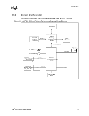
Introduction 1.3.3 System Configuration The following figures show typical platform configurations using the Intel® 820 chipset. Intel® 820 Chipset Platform Performance Desktop Block Diagram Processor 4X AGP Graphics Controller AGP 2.0 82820 Memory Controller Hub (MCH) Main Memory 4 IDE Drives 2 USB Ports Hub Interface PCI Bus PCI Slots AC'97 Codec(s) (optional) AC'97 2.1 82801AA I/O Controller Hub (ICH) Keyboard, Mouse, FD, PP, SP, IR LPC I/F Super I/O FWH Flash BIOS GPIO Intel®820 Chipset Design Guide 1-5 Figure 1-1.
Introduction 1.3.3 System Configuration The following figures show typical platform configurations using the Intel® 820 chipset. Intel® 820 Chipset Platform Performance Desktop Block Diagram Processor 4X AGP Graphics Controller AGP 2.0 82820 Memory Controller Hub (MCH) Main Memory 4 IDE Drives 2 USB Ports Hub Interface PCI Bus PCI Slots AC'97 Codec(s) (optional) AC'97 2.1 82801AA I/O Controller Hub (ICH) Keyboard, Mouse, FD, PP, SP, IR LPC I/F Super I/O FWH Flash BIOS GPIO Intel®820 Chipset Design Guide 1-5 Figure 1-1.

Design Guide
Page 20
... the PCI bus by the I /O features (IDE, AC'97, USB, etc.), receives adequate bandwidth. The powerdown mode of the 1.6 GB/s theoretical maximum bandwidth. The Pentium III processor new extensions complement the Intel MMX™ technology SIMD extensions and provide a performance boost to RDRAM's...allows graphics controllers to impact PCI bus performance. The RDRAM memory interface can achieve greater than 95% utilization of operation enables Intel® 820 chipset based systems to cost-effectively support suspend-to obtain optimal performance from the Pentium III processor as well ...
... the PCI bus by the I /O features (IDE, AC'97, USB, etc.), receives adequate bandwidth. The powerdown mode of the 1.6 GB/s theoretical maximum bandwidth. The Pentium III processor new extensions complement the Intel MMX™ technology SIMD extensions and provide a performance boost to RDRAM's...allows graphics controllers to impact PCI bus performance. The RDRAM memory interface can achieve greater than 95% utilization of operation enables Intel® 820 chipset based systems to cost-effectively support suspend-to obtain optimal performance from the Pentium III processor as well ...

Design Guide
Page 21
...CPU not booting) the ICH sends a message over the network to disable the following functions: AC'97 Modem, AC'97 Audio, IDE, USB or SMBus. SMBus The ICH integrates an SMBus controller. The SMBus provides an interface to an active INTRUDER# signal. In response to generate...be programmed to generate an SMI# or TCO interrupt due to manage peripherals (e.g., serial presence detection (SPD) on LAN*. Introduction 1.4.5 Manageability The Intel® 820 chipset platform integrates several messages to the ICH. TCO Timer The ICH integrates a programmable TCO Timer. CPU Present Indicator The ICH...
...CPU not booting) the ICH sends a message over the network to disable the following functions: AC'97 Modem, AC'97 Audio, IDE, USB or SMBus. SMBus The ICH integrates an SMBus controller. The SMBus provides an interface to an active INTRUDER# signal. In response to generate...be programmed to generate an SMI# or TCO interrupt due to manage peripherals (e.g., serial presence detection (SPD) on LAN*. Introduction 1.4.5 Manageability The Intel® 820 chipset platform integrates several messages to the ICH. TCO Timer The ICH integrates a programmable TCO Timer. CPU Present Indicator The ICH...

Design Guide
Page 23
...an integrated game port is required. In a system with ISA audio, the game port typically existed on system requirements, a device bay controller and USB hub could be integrated into the super I /O designs. For systems requiring ISA support, an ISA-IRQ to the LPC interface allows for a ...comprehensive list of devices offered and features supported. Intel®820 Chipset Design Guide 1-11 Migration to serial-IRQ converter is recommended because the AC'97 interface does not provide support for two...
...an integrated game port is required. In a system with ISA audio, the game port typically existed on system requirements, a device bay controller and USB hub could be integrated into the super I /O designs. For systems requiring ISA support, an ISA-IRQ to the LPC interface allows for a ...comprehensive list of devices offered and features supported. Intel®820 Chipset Design Guide 1-11 Migration to serial-IRQ converter is recommended because the AC'97 interface does not provide support for two...

Design Guide
Page 58
... and maximum trace length requirements as well as trace width and spacing requirements. INTA# - REQ# - AD_STB1# (used in 4X mode ONLY) Set #3 - USB- PERR# - WBF# - FRAME# - DEVSEL# • 2X/4X Timing Domain Set #1 - C/BE[1:0]# - PME# - However, trace length matching requirements...three groups: 1X timing domain signals, 2X/4X timing domain signals and miscellaneous signals. TRDY# - SB_STB - TYPDET# - INTB# Intel®820 Chipset Design Guide Layout/Routing Guidelines 2.7.1 2-32 AGP Interface Signal Groups The signals on the AGP interface are three sets ...
... and maximum trace length requirements as well as trace width and spacing requirements. INTA# - REQ# - AD_STB1# (used in 4X mode ONLY) Set #3 - USB- PERR# - WBF# - FRAME# - DEVSEL# • 2X/4X Timing Domain Set #1 - C/BE[1:0]# - PME# - However, trace length matching requirements...three groups: 1X timing domain signals, 2X/4X timing domain signals and miscellaneous signals. TRDY# - SB_STB - TYPDET# - INTB# Intel®820 Chipset Design Guide Layout/Routing Guidelines 2.7.1 2-32 AGP Interface Signal Groups The signals on the AGP interface are three sets ...
Design Guide
Page 68
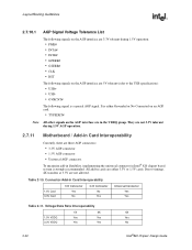
...USB+ • USB• OVRCNT# The following signal is strongly recommended. Connector/Add-in Card Interoperability Currently, there are three AGP connectors: • 3.3V AGP connector • 1.5V AGP connector • Universal AGP connector. Voltage/Data Rate Interoperability 1X 2X 4X 1.5V VDDQ Yes Yes Yes 3.3V VDDQ Yes Yes No 2-42 Intel... Tolerance List The following signals on the AGP interface are 3.3V tolerant during 1.5V AGP operation. 2.7.11 Motherboard / Add-in Card Interoperability 1.5V Card 3.3V Card 1.5V Connector Yes No 3.3V Connector No Yes Universal Connector Yes Yes...
...USB+ • USB• OVRCNT# The following signal is strongly recommended. Connector/Add-in Card Interoperability Currently, there are three AGP connectors: • 3.3V AGP connector • 1.5V AGP connector • Universal AGP connector. Voltage/Data Rate Interoperability 1X 2X 4X 1.5V VDDQ Yes Yes Yes 3.3V VDDQ Yes Yes No 2-42 Intel... Tolerance List The following signals on the AGP interface are 3.3V tolerant during 1.5V AGP operation. 2.7.11 Motherboard / Add-in Card Interoperability 1.5V Card 3.3V Card 1.5V Connector Yes No 3.3V Connector No Yes Universal Connector Yes Yes...

Design Guide
Page 91
data lines. • 15 Ω series resistors should be placed as close as possible to the ICH ( Layout/Routing Guidelines 2.15 USB The following are general guidelines for the USB interface: • Unused USB ports should be terminated with 15 KΩ pulldown resistors on both P+/P-
data lines. • 15 Ω series resistors should be placed as close as possible to the ICH ( Layout/Routing Guidelines 2.15 USB The following are general guidelines for the USB interface: • Unused USB ports should be terminated with 15 KΩ pulldown resistors on both P+/P-

Design Guide
Page 92
... during OS enumeration. 2.17 IOAPIC Design Recommendation UP systems not using the IOAPIC should follow these recommendations: • On the ICH - Layout/Routing Guidelines Recommended USB trace characteristics • Impedance 'Z0' = 45.4 Ω • Line Delay = 160.2 ps • Capacitance = 3.5 pF • Inductance = 7.3 nH •... the ICH to positively decode LPC cycles, and release the NOGO signal to ground through 10 KΩ resistors 2-66 Intel®820 Chipset Design Guide Connect PICCLK directly to subtractive decode. Since the LPC bridge logically sits on the PCI bus...
... during OS enumeration. 2.17 IOAPIC Design Recommendation UP systems not using the IOAPIC should follow these recommendations: • On the ICH - Layout/Routing Guidelines Recommended USB trace characteristics • Impedance 'Z0' = 45.4 Ω • Line Delay = 160.2 ps • Capacitance = 3.5 pF • Inductance = 7.3 nH •... the ICH to positively decode LPC cycles, and release the NOGO signal to ground through 10 KΩ resistors 2-66 Intel®820 Chipset Design Guide Connect PICCLK directly to subtractive decode. Since the LPC bridge logically sits on the PCI bus...
Design Guide
Page 129
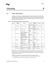
... N/A CLK66 CLK N/A 66 MHz 3.3V 2 REF[0-1] Internal ICH Logic ICH Internal Super I/O Logic Super I/O CLK14 Vendor Specific 14 MHz 3.3V 1 48 MHz USB ICH DRCG Reference Clock DRCG 2 CPU_DIV2[0-1] Unused N/A CLK48 REFCLK N/A 48 MHz 50/66 MHz 3.3V 2.5V The CK133 is important that meet the... for Routed to ensure the skew requirements are met between: • The MCH hub interface/AGP clock and the AGP connector (or device) Intel®820 Chipset Design Guide 4-1 Some of the output clocks are 3.3V and some of the system. The CK133 generates the clocks listed in...
... N/A CLK66 CLK N/A 66 MHz 3.3V 2 REF[0-1] Internal ICH Logic ICH Internal Super I/O Logic Super I/O CLK14 Vendor Specific 14 MHz 3.3V 1 48 MHz USB ICH DRCG Reference Clock DRCG 2 CPU_DIV2[0-1] Unused N/A CLK48 REFCLK N/A 48 MHz 50/66 MHz 3.3V 2.5V The CK133 is important that meet the... for Routed to ensure the skew requirements are met between: • The MCH hub interface/AGP clock and the AGP connector (or device) Intel®820 Chipset Design Guide 4-1 Some of the output clocks are 3.3V and some of the system. The CK133 generates the clocks listed in...

Design Guide
Page 154
...;820 Chipset Design Guide This power delivery architecture supports the "Instantly Available PC Design Guidelines" via 3.3V aux) and USB (USB can only be powered if sufficient standby power is accounted for the Intel® 820 Chipset Reference Board. The power requirements must be compared against the power budget supplied by the power supply...
...;820 Chipset Design Guide This power delivery architecture supports the "Instantly Available PC Design Guidelines" via 3.3V aux) and USB (USB can only be powered if sufficient standby power is accounted for the Intel® 820 Chipset Reference Board. The power requirements must be compared against the power budget supplied by the power supply...
Design Guide
Page 163
...System Bus Frequency - Floppy Disk Controller - 1 Parallel Port, 2 Serial Ports - APM Rev. 1.2 Compliant • Pentium III on-board VRM 8.4 compliant regulator • 4 Layer Design Intel®820 Chipset Design Guide A-1 Memory Controller Hub (MCH) - Via 4 REQ/GNT pairs (ICH supports 6 REQ#/GNT# pairs)... • AGP Universal Connector - 3.3V - 1X,2X signaling - 1.5V - 1X, 2X, 4X signaling • 2 IDE Connectors with Ultra ATA/66 Support • 2 USB ...
...System Bus Frequency - Floppy Disk Controller - 1 Parallel Port, 2 Serial Ports - APM Rev. 1.2 Compliant • Pentium III on-board VRM 8.4 compliant regulator • 4 Layer Design Intel®820 Chipset Design Guide A-1 Memory Controller Hub (MCH) - Via 4 REQ/GNT pairs (ICH supports 6 REQ#/GNT# pairs)... • AGP Universal Connector - 3.3V - 1X,2X signaling - 1.5V - 1X, 2X, 4X signaling • 2 IDE Connectors with Ultra ATA/66 Support • 2 USB ...

Design Guide
Page 164
... O UT O F PROPO SAL, SPECIFICATIO N OR SAM PLES. Intel products are subject to change. C urrent characterized errata are the property of their respective ow ners. 5 4 A TITLE: INTEL(R) 820 CHIPSET CUSTOMER REFERENCE BOARD REV: 1.01 R PCD PLATFORM DESIGN DRAWN BY: PROJECT: 1900... 2 1 INTEL(R) 820 CHIPSET UNIPROCESSOR CUSTOMER REFERENCE SCHEMATICS REV F (2 RIMM) D Title Cover Sheet Block Diagram Processor Connector Clock Synthesizer MCH ICH FWH C RIMM Sockets Super I/O A udio Audio/Modem Riser LAN Sy s tem A GP Connector PCI Connectors IDE Connectors B USB Connectors Parallel ...
... O UT O F PROPO SAL, SPECIFICATIO N OR SAM PLES. Intel products are subject to change. C urrent characterized errata are the property of their respective ow ners. 5 4 A TITLE: INTEL(R) 820 CHIPSET CUSTOMER REFERENCE BOARD REV: 1.01 R PCD PLATFORM DESIGN DRAWN BY: PROJECT: 1900... 2 1 INTEL(R) 820 CHIPSET UNIPROCESSOR CUSTOMER REFERENCE SCHEMATICS REV F (2 RIMM) D Title Cover Sheet Block Diagram Processor Connector Clock Synthesizer MCH ICH FWH C RIMM Sockets Super I/O A udio Audio/Modem Riser LAN Sy s tem A GP Connector PCI Connectors IDE Connectors B USB Connectors Parallel ...

Design Guide
Page 165
... DATA CTRL ADDR AGP AGP Bus MCH Rambus 2 RIMM Modules C IDE Primary UltraDMA/66 IDE Secondary PCI CNTRL USB Port 1 USB ICH PCI ADDR/DATA USB Port 2 LPC Bus AC'97 Audio Modem AC'97 Link B FWH 82559 LAN SIO Keyboard Mouse Floppy Parallel ... 7 C 16 93C46A 16 AD1881 13 CK133 5 DRCG 5 FWH 10 GD75232 25 LM4880 14 LPC47B27X 12 ADM1021 3 B TPS2042 23 A TITLE: INTEL(R) 820 CHIPSET CUSTOMER REFERENCE BOARD REV: BLOCK DIAGRAM 1.01 R PCD PLATFORM DESIGN DRAWN BY: PROJECT: 1900 PRAIRIE CITY ROAD FOLSOM, CALIFORNIA 95630 LAST REVISED: SHEET: 11-18...
... DATA CTRL ADDR AGP AGP Bus MCH Rambus 2 RIMM Modules C IDE Primary UltraDMA/66 IDE Secondary PCI CNTRL USB Port 1 USB ICH PCI ADDR/DATA USB Port 2 LPC Bus AC'97 Audio Modem AC'97 Link B FWH 82559 LAN SIO Keyboard Mouse Floppy Parallel ... 7 C 16 93C46A 16 AD1881 13 CK133 5 DRCG 5 FWH 10 GD75232 25 LM4880 14 LPC47B27X 12 ADM1021 3 B TPS2042 23 A TITLE: INTEL(R) 820 CHIPSET CUSTOMER REFERENCE BOARD REV: BLOCK DIAGRAM 1.01 R PCD PLATFORM DESIGN DRAWN BY: PROJECT: 1900 PRAIRIE CITY ROAD FOLSOM, CALIFORNIA 95630 LAST REVISED: SHEET: 11-18...

Design Guide
Page 172
... T4 LAD3/FWH3 T6 LDRQ0# N3 GPIO8/LDRQ1# U4 LFRAME#/FWH4 R1 USBP1+ P2 USBP1P1 USBP0+ N2 USBP0M4 OC1# M3 OC0# SYSTEM AC97 GPIO LPC USB ICH_B AC_SDATAOUT 9,13,15 8 7 6 5 4 3 VCC5_REF PDCS1# N12 SDCS1# L14 PDCS3# U13 SDCS3# L16 PDA0 PDA1 PDA2 SDA0 SDA1 SDA2 R12 T12 P12 M16... 22 22 22 22 22 PDD[15:0] SDD[15:0] C234 + 1UF 0.1UF R230 1K 1 VCC3_3 VCC5 +A -C D 22 22 C 22 B 22 A TITLE: INTEL(R) 820 CHIPSET CUSTOMER REFERENCE BOARD REV: ICH 1.01 R PCD PLATFORM DESIGN DRAWN BY: PROJECT: 1900 PRAIRIE CITY ROAD FOLSOM, CALIFORNIA 95630 LAST REVISED: SHEET: 12-2-1999_16:22 9 OF...
... T4 LAD3/FWH3 T6 LDRQ0# N3 GPIO8/LDRQ1# U4 LFRAME#/FWH4 R1 USBP1+ P2 USBP1P1 USBP0+ N2 USBP0M4 OC1# M3 OC0# SYSTEM AC97 GPIO LPC USB ICH_B AC_SDATAOUT 9,13,15 8 7 6 5 4 3 VCC5_REF PDCS1# N12 SDCS1# L14 PDCS3# U13 SDCS3# L16 PDA0 PDA1 PDA2 SDA0 SDA1 SDA2 R12 T12 P12 M16... 22 22 22 22 22 PDD[15:0] SDD[15:0] C234 + 1UF 0.1UF R230 1K 1 VCC3_3 VCC5 +A -C D 22 22 C 22 B 22 A TITLE: INTEL(R) 820 CHIPSET CUSTOMER REFERENCE BOARD REV: ICH 1.01 R PCD PLATFORM DESIGN DRAWN BY: PROJECT: 1900 PRAIRIE CITY ROAD FOLSOM, CALIFORNIA 95630 LAST REVISED: SHEET: 12-2-1999_16:22 9 OF...

Design Guide
Page 178
...A3 RESV[6] A4 RESV[7] A5 GND[7] A6 +5VDUAL/5VSBY A7 B8 GND[1] USB_OC A8 B9 +12V B10 GND[2] GND[8] A9 USB+ A10 B11 +5VD AC'97_RISER USB- A11 KEY KEY B12 GND[3] B13 RESV[3] B14 RESV[4] AMR_CONNECTOR KEY KEY GND[9] A12 S/P_DIF_IN A13 GND[10] A14 B15 ...13 AC97_OC# 23 AC97_USB+ 23 AC97_USB23 VCC3_3SBY R113 0K AC_SYNC 9,13 AC_SDATAIN1 9 AC_SDATAIN0 9,13 AC_BITCLK 9,13 1 D C B A A TITLE: INTEL(R) 820 CHIPSET CUSTOMER REFERENCE BOARD REV: AUDIO/MODEM RISER 1.01 R PCD PLATFORM DESIGN DRAWN BY: PROJECT: 1900 PRAIRIE CITY ROAD FOLSOM, CALIFORNIA 95630 LAST REVISED: SHEET: 15 OF...
...A3 RESV[6] A4 RESV[7] A5 GND[7] A6 +5VDUAL/5VSBY A7 B8 GND[1] USB_OC A8 B9 +12V B10 GND[2] GND[8] A9 USB+ A10 B11 +5VD AC'97_RISER USB- A11 KEY KEY B12 GND[3] B13 RESV[3] B14 RESV[4] AMR_CONNECTOR KEY KEY GND[9] A12 S/P_DIF_IN A13 GND[10] A14 B15 ...13 AC97_OC# 23 AC97_USB+ 23 AC97_USB23 VCC3_3SBY R113 0K AC_SYNC 9,13 AC_SDATAIN1 9 AC_SDATAIN0 9,13 AC_BITCLK 9,13 1 D C B A A TITLE: INTEL(R) 820 CHIPSET CUSTOMER REFERENCE BOARD REV: AUDIO/MODEM RISER 1.01 R PCD PLATFORM DESIGN DRAWN BY: PROJECT: 1900 PRAIRIE CITY ROAD FOLSOM, CALIFORNIA 95630 LAST REVISED: SHEET: 15 OF...

