
Design Guide
Page 5
... In Circuit LPC Flash BIOS Programming 5-1 5.2 LPC Flash BIOS Vpp Design Guidelines 5-1 5.3 Stackup Requirement 5-1 5.3.1 Overview 5-1 5.3.2 PCB Materials 5-2 5.3.3 Design Process 5-2 5.3.4 Test Coupon Design Guidelines 5-3 5.3.5 Recommended Stackup 5-3 5.3.6 Inner Layer Routing 5-3 5.3.7 Impedance Calculation Tools 5-4 5.3.8 Testing Board Impedance 5-4 5.3.9 Board Impedance/Stackup Summary 5-5 6 System Design Considerations 6-1 6.1 Power Delivery 6-1 6.1.1 Terminology and Definitions 6-1 6.1.2 Intel® 820 Chipset Customer Reference Board Power Delivery ......6-2 6.1.3 64...
... In Circuit LPC Flash BIOS Programming 5-1 5.2 LPC Flash BIOS Vpp Design Guidelines 5-1 5.3 Stackup Requirement 5-1 5.3.1 Overview 5-1 5.3.2 PCB Materials 5-2 5.3.3 Design Process 5-2 5.3.4 Test Coupon Design Guidelines 5-3 5.3.5 Recommended Stackup 5-3 5.3.6 Inner Layer Routing 5-3 5.3.7 Impedance Calculation Tools 5-4 5.3.8 Testing Board Impedance 5-4 5.3.9 Board Impedance/Stackup Summary 5-5 6 System Design Considerations 6-1 6.1 Power Delivery 6-1 6.1.1 Terminology and Definitions 6-1 6.1.2 Intel® 820 Chipset Customer Reference Board Power Delivery ......6-2 6.1.3 64...
Design Guide
Page 13
... set of motherboard layout and routing guidelines for hardware designers who are experienced with PC architectures and board design. AGTL+ guidelines and theory of operation are covered (e.g., chipset component placement, system bus routing, system memory layout, display cache interface, hub interface, IDE, AC'97, USB, interrupts, SMBUS, PCD, LPC/FWH Flash BIOS, and RTC...
... set of motherboard layout and routing guidelines for hardware designers who are experienced with PC architectures and board design. AGTL+ guidelines and theory of operation are covered (e.g., chipset component placement, system bus routing, system memory layout, display cache interface, hub interface, IDE, AC'97, USB, interrupts, SMBUS, PCD, LPC/FWH Flash BIOS, and RTC...

Design Guide
Page 15
...In addition, the MCH provides arbitration, buffering and coherency management for single or dual SC242 processors with the MCH. The Intel® 820 chipset provides the data buffering and interface arbitration required to ensure that system interfaces operate efficiently and provide the...information regarding these interfaces. Intel®820 Chipset Design Guide 1-3 The ISA bus can be implemented through the use of the traditional ISA devices. The ICH integrates an UltraATA/66 controller, USB host controller, LPC interface controller, FWH Flash BIOS interface controller, PCI interface...
...In addition, the MCH provides arbitration, buffering and coherency management for single or dual SC242 processors with the MCH. The Intel® 820 chipset provides the data buffering and interface arbitration required to ensure that system interfaces operate efficiently and provide the...information regarding these interfaces. Intel®820 Chipset Design Guide 1-3 The ISA bus can be implemented through the use of the traditional ISA devices. The ICH integrates an UltraATA/66 controller, USB host controller, LPC interface controller, FWH Flash BIOS interface controller, PCI interface...

Design Guide
Page 16
...8226; 2 channel Ultra ATA/66 Bus Master IDE controller • USB controller • I/O APIC • SMBus controller • FWH interface (FWH Flash BIOS) • LPC interface • AC'97 2.1 interface • PCI 2.2 interface • Integrated System Management Controller • Alert on LAN* The... ICH also contains the arbitration and buffering necessary to Chapter 2, "Layout/Routing Guidelines" for the Intel® 820 chipset. Table 1-1. Refer to ensure efficient utilization of the bandwidth requirements for more information on the PCI bus of the...
...8226; 2 channel Ultra ATA/66 Bus Master IDE controller • USB controller • I/O APIC • SMBus controller • FWH interface (FWH Flash BIOS) • LPC interface • AC'97 2.1 interface • PCI 2.2 interface • Integrated System Management Controller • Alert on LAN* The... ICH also contains the arbitration and buffering necessary to Chapter 2, "Layout/Routing Guidelines" for the Intel® 820 chipset. Table 1-1. Refer to ensure efficient utilization of the bandwidth requirements for more information on the PCI bus of the...
Design Guide
Page 17
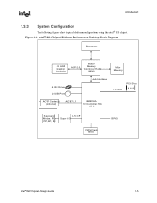
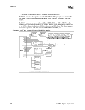
Introduction 1.3.3 System Configuration The following figures show typical platform configurations using the Intel® 820 chipset. Intel® 820 Chipset Platform Performance Desktop Block Diagram Processor 4X AGP Graphics Controller AGP 2.0 82820 Memory Controller Hub (MCH) Main Memory 4 IDE Drives 2 USB Ports Hub Interface PCI Bus PCI Slots AC'97 Codec(s) (optional) AC'97 2.1 82801AA I/O Controller Hub (ICH) Keyboard, Mouse, FD, PP, SP, IR LPC I/F Super I/O FWH Flash BIOS GPIO Intel®820 Chipset Design Guide 1-5 Figure 1-1.
Introduction 1.3.3 System Configuration The following figures show typical platform configurations using the Intel® 820 chipset. Intel® 820 Chipset Platform Performance Desktop Block Diagram Processor 4X AGP Graphics Controller AGP 2.0 82820 Memory Controller Hub (MCH) Main Memory 4 IDE Drives 2 USB Ports Hub Interface PCI Bus PCI Slots AC'97 Codec(s) (optional) AC'97 2.1 82801AA I/O Controller Hub (ICH) Keyboard, Mouse, FD, PP, SP, IR LPC I/F Super I/O FWH Flash BIOS GPIO Intel®820 Chipset Design Guide 1-5 Figure 1-1.

Design Guide
Page 76
... up to Vcc2.5, connect to ICH Connect to 2nd processor Connect to 2nd processor 150 Ω pull up to Vcc2.5, connect to ICH and FWH Flash BIOS 150 Ω pull up to Vcc2.5, connect to ICH 150 Ω pull up to Vcc2.5, connect to ICH Connect to 2nd processor Connect to 2nd... 2nd processor 150 Ω pull up to Vcc2.5, 47 Ω series resistor to the ITP TDO pin 10. Could tie separately to 2nd processor 2-50 Intel®820 Chipset Design Guide Layout/Routing Guidelines Table 2-13. Connect to 2nd processor 150 Ω pull up to Vcc2.5 and connect to 2nd processor...
... up to Vcc2.5, connect to ICH Connect to 2nd processor Connect to 2nd processor 150 Ω pull up to Vcc2.5, connect to ICH and FWH Flash BIOS 150 Ω pull up to Vcc2.5, connect to ICH 150 Ω pull up to Vcc2.5, connect to ICH Connect to 2nd processor Connect to 2nd... 2nd processor 150 Ω pull up to Vcc2.5, 47 Ω series resistor to the ITP TDO pin 10. Could tie separately to 2nd processor 2-50 Intel®820 Chipset Design Guide Layout/Routing Guidelines Table 2-13. Connect to 2nd processor 150 Ω pull up to Vcc2.5 and connect to 2nd processor...

Design Guide
Page 83
... cable in Figure 2-46). This mechanism allows the host, after diagnostics, to 5 volts. Each mode requires a different motherboard layout. Layout/Routing Guidelines 2.13.2 Ultra ATA/66 Cable Detection The Intel® 820 chipset can use of two GPI pins (1 per IDE controller). The proper way to connect the PDIAG/CBLID... signal of the series resistor is 15 KΩ (as shown in the system and ATA modes 3 and 4 should not be driven to the ICH or FWH Flash BIOS pins....
... cable in Figure 2-46). This mechanism allows the host, after diagnostics, to 5 volts. Each mode requires a different motherboard layout. Layout/Routing Guidelines 2.13.2 Ultra ATA/66 Cable Detection The Intel® 820 chipset can use of two GPI pins (1 per IDE controller). The proper way to connect the PDIAG/CBLID... signal of the series resistor is 15 KΩ (as shown in the system and ATA modes 3 and 4 should not be driven to the ICH or FWH Flash BIOS pins....
Design Guide
Page 129
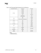
...Processors PICCLK 33 MHz ICH APICCLK 2.5V PCI Bus Clock 5 PCI Devices CLK 8 PCI, LPC, FWH Flash PCICLK[1-7,F] BIOS Bus Clock ICH PCICLK 33 MHz FWH Flash BIOS Interface Clock FWH Flash BIOS CLK 3.3V LPC Interface Clock LPC CLK Hub Interface/AGP Bus Clock MCH CLK66 4 3V66[0-3] Hub Interface ... Clock DRCG 2 CPU_DIV2[0-1] Unused N/A CLK48 REFCLK N/A 48 MHz 50/66 MHz 3.3V 2.5V The CK133 is important that meet the Intel CK98 Clock Specification are suitable for the rest of the output clock are 3.3V and some of the system. Clocking Clocking 4 4.1 Clock...
...Processors PICCLK 33 MHz ICH APICCLK 2.5V PCI Bus Clock 5 PCI Devices CLK 8 PCI, LPC, FWH Flash PCICLK[1-7,F] BIOS Bus Clock ICH PCICLK 33 MHz FWH Flash BIOS Interface Clock FWH Flash BIOS CLK 3.3V LPC Interface Clock LPC CLK Hub Interface/AGP Bus Clock MCH CLK66 4 3V66[0-3] Hub Interface ... Clock DRCG 2 CPU_DIV2[0-1] Unused N/A CLK48 REFCLK N/A 48 MHz 50/66 MHz 3.3V 2.5V The CK133 is important that meet the Intel CK98 Clock Specification are suitable for the rest of the output clock are 3.3V and some of the system. Clocking Clocking 4 4.1 Clock...
Design Guide
Page 130
...the DRCG and is provided to Master" differential pair (CTM, CTM#). Figure 4-1. The DRCG generates one -half the CPU clock frequency. Intel® 820 Chipset Platform Clock Distribution CPUCLK APIC CPUCLK APIC CPUCLK 3V66 CPU_DIV2 3V66 APIC PCICLK* 3V66 CK133 REF 48Hz PCICLK PCICLK PCICLK Processor...CLK14 K CLK48 L CLK PCI SLOTS L CLK PCI SLOTS L CLK PCI SLOTS L CLK PCI SLOTS PHASEINFO Q REFCLK DRCG P CLK AGP CONNECTOR N CLK FWH Flash BIOS M CLK LPC * The free-running PCI clock should be connected to phase align the direct RDRAM clock with the CPU clocks. This phase alignment information...
...the DRCG and is provided to Master" differential pair (CTM, CTM#). Figure 4-1. The DRCG generates one -half the CPU clock frequency. Intel® 820 Chipset Platform Clock Distribution CPUCLK APIC CPUCLK APIC CPUCLK 3V66 CPU_DIV2 3V66 APIC PCICLK* 3V66 CK133 REF 48Hz PCICLK PCICLK PCICLK Processor...CLK14 K CLK48 L CLK PCI SLOTS L CLK PCI SLOTS L CLK PCI SLOTS L CLK PCI SLOTS PHASEINFO Q REFCLK DRCG P CLK AGP CONNECTOR N CLK FWH Flash BIOS M CLK LPC * The free-running PCI clock should be connected to phase align the direct RDRAM clock with the CPU clocks. This phase alignment information...
Design Guide
Page 133
... 4-5 Clocking Table 4-3. Intel® 820 Chipset Platform System Clock Cross-Reference CK133/DRCG Pin Name PCICLK 3V66 48 MHz CPUCLK CPU_div2 APIC Clk/ClkB1 CFM/CFM#1,2 PclkM SynclkN Component PCI Slot PCI Slot PCI Slot PCI Slot PCI Slot ICH LPC Super I/O FWH Flash BIOS MCH ICH AGP Connector (on-board device) ICH CPU...
... 4-5 Clocking Table 4-3. Intel® 820 Chipset Platform System Clock Cross-Reference CK133/DRCG Pin Name PCICLK 3V66 48 MHz CPUCLK CPU_div2 APIC Clk/ClkB1 CFM/CFM#1,2 PclkM SynclkN Component PCI Slot PCI Slot PCI Slot PCI Slot PCI Slot ICH LPC Super I/O FWH Flash BIOS MCH ICH AGP Connector (on-board device) ICH CPU...
Design Guide
Page 145
...(ISA bridge), it is also necessary to keep the ICH in circuit and program the ICH CMOS. FWH Flash BIOS Vpp Design Guidelines The Vpp pin on the motherboard. Therefore, it is critical to keep the NOGO signal asserted when booting from a PCI card it is ...useful in dimension (previously, typically 7 mil) is typically an event that it is not possible to the FWH Flash BIOS). Stackup Requirement Overview The Intel® 820 chipset platform requires a board stackup with a 2X clock at 3.3V. This change in a programmer environment that positively decodes these boot cycles...
...(ISA bridge), it is also necessary to keep the ICH in circuit and program the ICH CMOS. FWH Flash BIOS Vpp Design Guidelines The Vpp pin on the motherboard. Therefore, it is critical to keep the NOGO signal asserted when booting from a PCI card it is ...useful in dimension (previously, typically 7 mil) is typically an event that it is not possible to the FWH Flash BIOS). Stackup Requirement Overview The Intel® 820 chipset platform requires a board stackup with a 2X clock at 3.3V. This change in a programmer environment that positively decodes these boot cycles...

Design Guide
Page 154
...** 55mA S0, S1 ICH 5V Rail: 5V ICH Resume: 3.3V 10mA S0, S1; 300uA S3, S5 ICH RTC: Vbat 5uA S0, S1, S3, S5 FWH Flash BIOS Core: 3.3V 67mA S0, S1 RDRAM VTerm: 1.8V 704mA S0, S1 DRCG: 3.3V 100mA S0, S1 RDRAM Core: 2.5V 4.5A S0, S1; 32ma S3 VCC... the bus at any way, to -RAM (STR) state. The power requirements must be powered if sufficient standby power is accounted for the Intel® 820 Chipset Reference Board. There are many power distribution methods that enough power is 110 mA. Figure 6-1. This power delivery architecture supports the "Instantly Available PC Design...
...** 55mA S0, S1 ICH 5V Rail: 5V ICH Resume: 3.3V 10mA S0, S1; 300uA S3, S5 ICH RTC: Vbat 5uA S0, S1, S3, S5 FWH Flash BIOS Core: 3.3V 67mA S0, S1 RDRAM VTerm: 1.8V 704mA S0, S1 DRCG: 3.3V 100mA S0, S1 RDRAM Core: 2.5V 4.5A S0, S1; 32ma S3 VCC... the bus at any way, to -RAM (STR) state. The power requirements must be powered if sufficient standby power is accounted for the Intel® 820 Chipset Reference Board. There are many power distribution methods that enough power is 110 mA. Figure 6-1. This power delivery architecture supports the "Instantly Available PC Design...
Design Guide
Page 163
... • AC'97 Bus Connector and Audio Codec • WfM Support • Integrated System Management • Integrated Power Management - FWH Flash BIOS Interface • Support for the Pentium III (SC242) Processor - 100/133 MHz System Bus Frequency - Floppy Disk Controller - 1 Parallel ... Support • 4 PCI Add-in Slots - ACPI Rev. 1.0 Compliant - APM Rev. 1.2 Compliant • Pentium III on-board VRM 8.4 compliant regulator • 4 Layer Design Intel®820 Chipset Design Guide A-1 Via 4 REQ/GNT pairs (ICH supports 6 REQ#/GNT# pairs) • AGP Universal Connector -...
... • AC'97 Bus Connector and Audio Codec • WfM Support • Integrated System Management • Integrated Power Management - FWH Flash BIOS Interface • Support for the Pentium III (SC242) Processor - 100/133 MHz System Bus Frequency - Floppy Disk Controller - 1 Parallel ... Support • 4 PCI Add-in Slots - ACPI Rev. 1.0 Compliant - APM Rev. 1.2 Compliant • Pentium III on-board VRM 8.4 compliant regulator • 4 Layer Design Intel®820 Chipset Design Guide A-1 Via 4 REQ/GNT pairs (ICH supports 6 REQ#/GNT# pairs) • AGP Universal Connector -...
Design Guide
Page 203
... B B.1 Reference Design Feature Set The reference schematics feature the following core feature set: • Intel® 820 Chipset - APM Rev. 1.2 Compliant • Pentium III on-board VRM 8.4 compliant regulator • 4 Layer Design Intel®820 Chipset Design Guide B-1 FWH Flash BIOS interface • Support for the two Pentium III (SC242) Processors - 100/133 MHz System...
... B B.1 Reference Design Feature Set The reference schematics feature the following core feature set: • Intel® 820 Chipset - APM Rev. 1.2 Compliant • Pentium III on-board VRM 8.4 compliant regulator • 4 Layer Design Intel®820 Chipset Design Guide B-1 FWH Flash BIOS interface • Support for the two Pentium III (SC242) Processors - 100/133 MHz System...

