Design Guide
Page 14
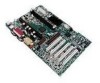
...administration and troubleshooting. This removes many of the conflicts experienced when installing hardware and drivers into the I /O Controller Hub Datasheet (Order Number: 290655) • Intel® 82802AB/82802AC FirmWare Hub (FWH) Datasheet (Order Number: 290658) &#...Intel® 820 Chipset: Intel® 82820 Memory Controller Hub (MCH) Datasheet (Order Number: 290630) • Intel® 82801AA (ICH) and Intel® 82801AB (ICH0) I /O subsystem of Intel chipsets. A new chipset component interconnect, the hub interface, is the third generation desktop chipset designed for the Intel...
...administration and troubleshooting. This removes many of the conflicts experienced when installing hardware and drivers into the I /O Controller Hub Datasheet (Order Number: 290655) • Intel® 82802AB/82802AC FirmWare Hub (FWH) Datasheet (Order Number: 290658) &#...Intel® 820 Chipset: Intel® 82820 Memory Controller Hub (MCH) Datasheet (Order Number: 290630) • Intel® 82801AA (ICH) and Intel® 82801AB (ICH0) I /O subsystem of Intel chipsets. A new chipset component interconnect, the hub interface, is the third generation desktop chipset designed for the Intel...

Design Guide
Page 77
...- 33 Ω series resistor (Though OEM needs to simulate based on -board VR or VRM. Zero ohm resistors are an option instead of the VR)..... May also connect to 1.5V regulator. Connect to system monitoring device. This checklist supports Intel® Pentium® II processors at the clock driver then route to CK133 SEL133/100# pin. Terminate as noconnects: A16, A47, A88, ...in same manner as CPU0. Implement in same manner as CPU0. Connect to MCH HL10 pin Connect to on driver characteristics) Use separate BCLK from TAP and CPU0, or use a 1 KΩ - 10 KΩ pull...
...- 33 Ω series resistor (Though OEM needs to simulate based on -board VR or VRM. Zero ohm resistors are an option instead of the VR)..... May also connect to 1.5V regulator. Connect to system monitoring device. This checklist supports Intel® Pentium® II processors at the clock driver then route to CK133 SEL133/100# pin. Terminate as noconnects: A16, A47, A88, ...in same manner as CPU0. Implement in same manner as CPU0. Connect to MCH HL10 pin Connect to on driver characteristics) Use separate BCLK from TAP and CPU0, or use a 1 KΩ - 10 KΩ pull...

Design Guide
Page 89
...Intel® 820 chipset platform, the ICH supports Wake on the link via the AC'97 link. AC'97 SDIN Pulldown Resistors System Solution On-board Codec Only AMR Only BOTH AMR and On-board Codec Pullup Requirements Pulldown the SDIN pin that is NOT connected to the primary codec vendor for board... to compensate for the implementation of 50pF. 2.14.2 AC'97 Motherboard Implementation The following design considerations are no AMR), then the unused ... it implies that could be driven. A series resistor at the driver and a capacitor at least one codec. These design guidelines have...
...Intel® 820 chipset platform, the ICH supports Wake on the link via the AC'97 link. AC'97 SDIN Pulldown Resistors System Solution On-board Codec Only AMR Only BOTH AMR and On-board Codec Pullup Requirements Pulldown the SDIN pin that is NOT connected to the primary codec vendor for board... to compensate for the implementation of 50pF. 2.14.2 AC'97 Motherboard Implementation The following design considerations are no AMR), then the unused ... it implies that could be driven. A series resistor at the driver and a capacitor at least one codec. These design guidelines have...

Design Guide
Page 91
Layout/Routing Guidelines 2.15 USB The following are general guidelines for the USB interface: • Unused USB ports should be terminated with 15 KΩ pulldown resistors on both P+/P- data lines. • 15 Ω series resistors should be placed as close as possible to the ICH (
Layout/Routing Guidelines 2.15 USB The following are general guidelines for the USB interface: • Unused USB ports should be terminated with 15 KΩ pulldown resistors on both P+/P- data lines. • 15 Ω series resistors should be placed as close as possible to the ICH (

Design Guide
Page 101
...corner is a step-by -step methodology. This is expected to output time, output driver edge rate, output drive current, and input drive current. This section also includes equations... 3 3.1 Section 2.9, "System Bus Design" on page 2-46 describes the recommendations for designing Intel® 820 chipset based platforms. This chapter discusses more details and insights. Section 3.4, "More...Logic. Similar discussion of components that transmits a coupled signal to design high performance desktop systems. Section 3.3, "Theory" on page 3-15 introduces the theories that are open...
...corner is a step-by -step methodology. This is expected to output time, output driver edge rate, output drive current, and input drive current. This section also includes equations... 3 3.1 Section 2.9, "System Bus Design" on page 2-46 describes the recommendations for designing Intel® 820 chipset based platforms. This chapter discusses more details and insights. Section 3.4, "More...Logic. Similar discussion of components that transmits a coupled signal to design high performance desktop systems. Section 3.3, "Theory" on page 3-15 introduces the theories that are open...

Design Guide
Page 102
... effects. • The Maximum Flight Time is switching. • Odd Mode Cross-talk - For more obvious causes include variation of the board dielectric constant, changes in load condition, crosstalk, VTT noise, VREF noise, variation in termination resistance and differences in the opposite direction that may...; Pro processor. See Section for more details of GTL+. 3-2 Intel®820 Chipset Design Guide See the definition of the driver, plus any adjustments to the SC242 connector. This is an enhancement to specify the driver's AC timings. It is an incident wave switching, open-drain ...
... effects. • The Maximum Flight Time is switching. • Odd Mode Cross-talk - For more obvious causes include variation of the board dielectric constant, changes in load condition, crosstalk, VTT noise, VREF noise, variation in termination resistance and differences in the opposite direction that may...; Pro processor. See Section for more details of GTL+. 3-2 Intel®820 Chipset Design Guide See the definition of the driver, plus any adjustments to the SC242 connector. This is an enhancement to specify the driver's AC timings. It is an incident wave switching, open-drain ...

Design Guide
Page 103
...defined above and below VSS at the processor core pad. Advanced System Bus Design Term Definition Network The trace of a Printed Circuit Board (PCB) that may cause additional propagation delay (or "pushout"), or a decrease in propagation delay (or "pull-in"). Overshoot ...SSO) Effects Refers to the difference in electrical timing parameters and degradation in simulation. Intel®820 Chipset Design Guide 3-3 Intel uses a 50 Ω test load for a signal to reflections, driver oscillations, etc. Maximum voltage allowed for specifying its maximum absolute value. Pin A...
...defined above and below VSS at the processor core pad. Advanced System Bus Design Term Definition Network The trace of a Printed Circuit Board (PCB) that may cause additional propagation delay (or "pushout"), or a decrease in propagation delay (or "pull-in"). Overshoot ...SSO) Effects Refers to the difference in electrical timing parameters and degradation in simulation. Intel®820 Chipset Design Guide 3-3 Intel uses a 50 Ω test load for a signal to reflections, driver oscillations, etc. Maximum voltage allowed for specifying its maximum absolute value. Pin A...

Design Guide
Page 106
...Intel® Pentium® III processor core at the pins. TSU_MIN = 1.9 ns assumes the 82820 MCH sees a minimum edge rate equal to offset the degradation caused by SSO push-out and other than those listed above must be set to calculate the expected signal propagation rate of a board...+ initial maximum flight time and Table 3-3 is set at 60 Ω ±15% Table 3-1 lists the AGTL+ component timings of driver and receiver. The commonly used "textbook" equations used . Table 3-1. Please check the appropriate component documentation for a 133 MHz, 2-way Pentium III processor...
...Intel® Pentium® III processor core at the pins. TSU_MIN = 1.9 ns assumes the 82820 MCH sees a minimum edge rate equal to offset the degradation caused by SSO push-out and other than those listed above must be set to calculate the expected signal propagation rate of a board...+ initial maximum flight time and Table 3-3 is set at 60 Ω ±15% Table 3-1 lists the AGTL+ component timings of driver and receiver. The commonly used "textbook" equations used . Table 3-1. Please check the appropriate component documentation for a 133 MHz, 2-way Pentium III processor...

Design Guide
Page 107
... (stripline or microstrip). • The length of the trace and the load of clock driver skew if outputs are not tied together and a clock driver that the board propagation constant multiplied by the multi-bit adjustment factor and should be covered by the trace ... time. 4. Cross-talk on the baseboard design and additional adjustment factors or margins are examples only. See the appropriate Intel 820 chipset documentation for 133 MHz Bus1 Driver Processor4 Processor4 82820 MCH Receiver Processor4 82820 MCH Processor4 Clk Period2 7.50 7.50 7.50 TCO_MAX 2.7 2.7 3.63 TSU_MIN ...
... (stripline or microstrip). • The length of the trace and the load of clock driver skew if outputs are not tied together and a clock driver that the board propagation constant multiplied by the multi-bit adjustment factor and should be covered by the trace ... time. 4. Cross-talk on the baseboard design and additional adjustment factors or margins are examples only. See the appropriate Intel 820 chipset documentation for 133 MHz Bus1 Driver Processor4 Processor4 82820 MCH Receiver Processor4 82820 MCH Processor4 Clk Period2 7.50 7.50 7.50 TCO_MAX 2.7 2.7 3.63 TSU_MIN ...

Design Guide
Page 108
... regions meet timing and signal quality specifications. Outputs from each sweep should be analyzed systematically. Example TFLT_MIN Calculations (Frequency Independent) Driver Processor2 Processor2 82820 MCH Receiver Processor2 82820 MCH Processor2 THOLD 0.8 0.28 0.8 ClkSKEW 0.2 0.2 0.2 TCO_MIN -0.1 -0.1 0.5 Recommended... signal quality requirements. By basing board layout guidelines on page 2-46). 3.2.3 Pre-Layout Simulation 3.2.3.1 3.2.3.2 Methodology Analog simulations are based on pre-layout simulations conducted at Intel. The layout recommendations in passing timing...
... regions meet timing and signal quality specifications. Outputs from each sweep should be analyzed systematically. Example TFLT_MIN Calculations (Frequency Independent) Driver Processor2 Processor2 82820 MCH Receiver Processor2 82820 MCH Processor2 THOLD 0.8 0.28 0.8 ClkSKEW 0.2 0.2 0.2 TCO_MIN -0.1 -0.1 0.5 Recommended... signal quality requirements. By basing board layout guidelines on page 2-46). 3.2.3 Pre-Layout Simulation 3.2.3.1 3.2.3.2 Methodology Analog simulations are based on pre-layout simulations conducted at Intel. The layout recommendations in passing timing...

Design Guide
Page 109
...must be approximately 1 Ω*mil2/inch, not the 0.662 Ω*mil2/inch value for annealed copper that drivers located in all driver locations, and analyzing each possible driver. For the example topology, vary the following parameters during Monte Carlo simulations: • Lengths L1 through L3 &#... corner is needed because the buffer's drive capability will be placed between the output of a receiver model. Intel®820 Chipset Design Guide 3-9 Positioning drivers with both rising and falling edge transitions. The fast corner is needed because the fast edge rate creates the...
...must be approximately 1 Ω*mil2/inch, not the 0.662 Ω*mil2/inch value for annealed copper that drivers located in all driver locations, and analyzing each possible driver. For the example topology, vary the following parameters during Monte Carlo simulations: • Lengths L1 through L3 &#... corner is needed because the buffer's drive capability will be placed between the output of a receiver model. Intel®820 Chipset Design Guide 3-9 Positioning drivers with both rising and falling edge transitions. The fast corner is needed because the fast edge rate creates the...

Design Guide
Page 112
...from the processor edge to compensate for this topology. Host Clock Routing Clock Net Trace length Clock driver to SC242 connector Clock driver to Intel 82820 MCH H H + (clock delay from the clock driver output pin and ending at the SC242 connector BCLK pin. PICD[1,0] Uni-Processor Topology 2.5V...8486; resistors. PICD[1,0] Dual-Processor Topology 2.5V 330 Ω L1 Intel® 820 Chipset: ICH SC242 L(1): Z0=60 Ω ±15%. Note that the clock route from the clock driver to the Intel 82820 MCH will require an additional trace length of the host clock trace...
...from the processor edge to compensate for this topology. Host Clock Routing Clock Net Trace length Clock driver to SC242 connector Clock driver to Intel 82820 MCH H H + (clock delay from the clock driver output pin and ending at the SC242 connector BCLK pin. PICD[1,0] Uni-Processor Topology 2.5V...8486; resistors. PICD[1,0] Dual-Processor Topology 2.5V 330 Ω L1 Intel® 820 Chipset: ICH SC242 L(1): Z0=60 Ω ±15%. Note that the clock route from the clock driver to the Intel 82820 MCH will require an additional trace length of the host clock trace...

Design Guide
Page 113
...Intel has shown that sensitivity analysis dramatically reduces the amount of "tuning" may not settle to the minimum VOL before the next rising edge is needed. Intersymbol Interference Intersymbol Interference (ISI) refers to the distortion or change in subsequent cycles. When the driver...take into consideration. Instead, baseboard lengths should take these conditions into account the expected variation for all parameters recommended for the board from the CAD layout tools. Evaluate both odd and even mode cross-talk conditions. Advanced System Bus Design 3.2.5 3.2.5.1 ...
...Intel has shown that sensitivity analysis dramatically reduces the amount of "tuning" may not settle to the minimum VOL before the next rising edge is needed. Intersymbol Interference Intersymbol Interference (ISI) refers to the distortion or change in subsequent cycles. When the driver...take into consideration. Instead, baseboard lengths should take these conditions into account the expected variation for all parameters recommended for the board from the CAD layout tools. Evaluate both odd and even mode cross-talk conditions. Advanced System Bus Design 3.2.5 3.2.5.1 ...

Design Guide
Page 114
...and is equal to the pin, it driving a test load. Actual System Load CLK I/O Buffer Vcc Driver Pad D SETQ VTT RTEST Test Load Driver Pin CLR Q TREF TCO CLK I/O Buffer Vcc Driver Pad D SETQ CLR Q Actual System Load VTT RTT Receiver Pin TFLIGHTSYSTEM Figure 3-3 above shows the ...to the I /O buffer. Controlling the temperature and voltage to correspond to avoid 3-14 Intel®820 Chipset Design Guide Test Load vs. The flip-flop represents the logic input and driver stage of the component. Advanced System Bus Design 3.2.6 Validation Build systems and validate the ...
...and is equal to the pin, it driving a test load. Actual System Load CLK I/O Buffer Vcc Driver Pad D SETQ VTT RTEST Test Load Driver Pin CLR Q TREF TCO CLK I/O Buffer Vcc Driver Pad D SETQ CLR Q Actual System Load VTT RTT Receiver Pin TFLIGHTSYSTEM Figure 3-3 above shows the ...to the I /O buffer. Controlling the temperature and voltage to correspond to avoid 3-14 Intel®820 Chipset Design Guide Test Load vs. The flip-flop represents the logic input and driver stage of the component. Advanced System Bus Design 3.2.6 Validation Build systems and validate the ...

Design Guide
Page 115
... pertaining to the driver-system interface and the same is satisfied: Equation 3-5. Valid Delay Equation Valid Delay = TCO + TFLIGHT-SYS - TREF must be generated using the same test load for the processor bus. In this timing value in the AGTL+ I/O buffer models. Intel®820 Chipset ...do not need TREF correction since these are the actual numbers. Intel provides this manner, the following valid delay equation is true for the driver output pin to reach the measurement voltage, VREF, starting from when the driver sees a valid clock pulse to the time when the receiver ...
... pertaining to the driver-system interface and the same is satisfied: Equation 3-5. Valid Delay Equation Valid Delay = TCO + TFLIGHT-SYS - TREF must be generated using the same test load for the processor bus. In this timing value in the AGTL+ I/O buffer models. Intel®820 Chipset ...do not need TREF correction since these are the actual numbers. Intel provides this manner, the following valid delay equation is true for the driver output pin to reach the measurement voltage, VREF, starting from when the driver sees a valid clock pulse to the time when the receiver ...

Design Guide
Page 116
...the system clock generation and distribution. • Changes in personal computer designs. Figure 3-4 shows a driver on the aggressor network and a receiver on the victim network. 3-16 Intel®820 Chipset Design Guide This requires that designers using AGTL+ be the same as the aggressor's ... TCO in the system. • The amount of the network. Cross-talk is dependent on many things. This includes: - The board loading impact on the aggressor's network. Advanced System Bus Design 3.3.2 3.3.3 Timing Requirements The system timing for AGTL+ is caused through capacitive...
...the system clock generation and distribution. • Changes in personal computer designs. Figure 3-4 shows a driver on the aggressor network and a receiver on the victim network. 3-16 Intel®820 Chipset Design Guide This requires that designers using AGTL+ be the same as the aggressor's ... TCO in the system. • The amount of the network. Cross-talk is dependent on many things. This includes: - The board loading impact on the aggressor's network. Advanced System Bus Design 3.3.2 3.3.3 Timing Requirements The system timing for AGTL+ is caused through capacitive...

Design Guide
Page 118
... may not be suitable. These networks have acceptable characteristics. 3-18 Intel®820 Chipset Design Guide and 20-pin components). Intel recommends using discrete resistors, resistor networks with a resistor network vendor ...pulses from 0% to double. Advanced System Bus Design 3.3.3.1 propagation time on two sides of a driver. This can cause the voltage (noise) from segments on the coupled network length exceeds one half... voltage swing, and the fall time is 3 V/ns and board delay is 175 ps/inch (2.1 ns/foot): Fall time = 1.5 V÷3 V/ns = 0.5 ns Length...
... may not be suitable. These networks have acceptable characteristics. 3-18 Intel®820 Chipset Design Guide and 20-pin components). Intel recommends using discrete resistors, resistor networks with a resistor network vendor ...pulses from 0% to double. Advanced System Bus Design 3.3.3.1 propagation time on two sides of a driver. This can cause the voltage (noise) from segments on the coupled network length exceeds one half... voltage swing, and the fall time is 3 V/ns and board delay is 175 ps/inch (2.1 ns/foot): Fall time = 1.5 V÷3 V/ns = 0.5 ns Length...
Design Guide
Page 123
... planes would be a good compromise. The system clock skew must be evaluated to ensure these general guidelines: • Tie clock driver outputs if clock buffer supports this document have different propagation velocities). • Maintain consistent impedance for the clock traces. - Minimize ...) on the primary and secondary sides. • Minimize serpentine traces on outer layers. Advanced System Bus Design 3.4.3.4 3.4.4 SC242 Connector Intel studies indicate that the use of layers the clocks are routed on, the smaller the impedance difference between each trace is likely to ...
... planes would be a good compromise. The system clock skew must be evaluated to ensure these general guidelines: • Tie clock driver outputs if clock buffer supports this document have different propagation velocities). • Maintain consistent impedance for the clock traces. - Minimize ...) on the primary and secondary sides. • Minimize serpentine traces on outer layers. Advanced System Bus Design 3.4.3.4 3.4.4 SC242 Connector Intel studies indicate that the use of layers the clocks are routed on, the smaller the impedance difference between each trace is likely to ...

Design Guide
Page 124
Since VTT is specified with a small timing error penalty. Timings are documented in the clock trace.) Definitions of the driver and receiver, while signal integrity is shifted by ∆VREF for a high-to within 200 mV of each clock ensures a low ...times. This places the absolute ringback limits at the pad violates the following noise sources: • Motherboard coupling • VTT noise • VREF noise Ringback Levels The example topology covered in the Intel® Pentium® II Processor Developer's Manual. ringback are measured at the pins of Flight Time...
Since VTT is specified with a small timing error penalty. Timings are documented in the clock trace.) Definitions of the driver and receiver, while signal integrity is shifted by ∆VREF for a high-to within 200 mV of each clock ensures a low ...times. This places the absolute ringback limits at the pad violates the following noise sources: • Motherboard coupling • VTT noise • VREF noise Ringback Levels The example topology covered in the Intel® Pentium® II Processor Developer's Manual. ringback are measured at the pins of Flight Time...

Design Guide
Page 125
... to take into Test Load VREF+ 200 mV VVRREEFF-+1100V0R0EmmF VV∆VREF ∆VREF Overdrive Regio VREF Guardband Tflight-max Tflight-min Intel®820 Chipset Design Guide 3-25 So, for a rising edge is bounded by VREF-∆VREF and VREF+∆VREF. Figure 3-11.... The minimum flight time for maximum rising edge correction, extrapolate back to VREF - ∆VREF. This region is measured from the time the driver crosses VREF when terminated to a test load, to the appropriate VREF Guardband boundary, and not VREF. Figure 3-12. Advanced System Bus Design should...
... to take into Test Load VREF+ 200 mV VVRREEFF-+1100V0R0EmmF VV∆VREF ∆VREF Overdrive Regio VREF Guardband Tflight-max Tflight-min Intel®820 Chipset Design Guide 3-25 So, for a rising edge is bounded by VREF-∆VREF and VREF+∆VREF. Figure 3-11.... The minimum flight time for maximum rising edge correction, extrapolate back to VREF - ∆VREF. This region is measured from the time the driver crosses VREF when terminated to a test load, to the appropriate VREF Guardband boundary, and not VREF. Figure 3-12. Advanced System Bus Design should...


