

Service Manual
Page 3
...as follows - Canada (CSA); Switzerland (SEV); VINC COPYRIGHT © 2000 V, INC. Service Manual VIZIO P42HDTV10A IBM and IBM products are registered trademarks of the following measures -- Macintosh and Power Macintosh are registered trademarks of Apple Computer, Inc. and VINC. products are registered trademarks of V, Inc.... in accordance with bonded ferrite cores. increase the separation between equipment and receiver; SAFETY CAUTION Use a power cable that meets the local safety standards. Japan (Electric Appliance Control Act); VIZIO P42HDTV10A Service Manual
...as follows - Canada (CSA); Switzerland (SEV); VINC COPYRIGHT © 2000 V, INC. Service Manual VIZIO P42HDTV10A IBM and IBM products are registered trademarks of the following measures -- Macintosh and Power Macintosh are registered trademarks of Apple Computer, Inc. and VINC. products are registered trademarks of V, Inc.... in accordance with bonded ferrite cores. increase the separation between equipment and receiver; SAFETY CAUTION Use a power cable that meets the local safety standards. Japan (Electric Appliance Control Act); VIZIO P42HDTV10A Service Manual

Service Manual
Page 5
... Inputs 6 x Stereo RCA (R/L), 1 x PC Mini-Jack Audio Outputs Analog - 1 x stereo RCA (R/L) 1 x headphone Digital - 1 x SPDIF Optical Audio 10W 6Ω X 2 Power Input 100 to 240 Vac Power Consumption 380W Max Preset Modes Primary 1024 x 768 @ 60Hz. TV system NTSC/ATSC/ QAM PC Inputs 15pins D-sub, HDMI-DVI Video Inputs 1 x S-Video 3 x AV inputs (CVBS; Chapter 2 Specification 1.
... Inputs 6 x Stereo RCA (R/L), 1 x PC Mini-Jack Audio Outputs Analog - 1 x stereo RCA (R/L) 1 x headphone Digital - 1 x SPDIF Optical Audio 10W 6Ω X 2 Power Input 100 to 240 Vac Power Consumption 380W Max Preset Modes Primary 1024 x 768 @ 60Hz. TV system NTSC/ATSC/ QAM PC Inputs 15pins D-sub, HDMI-DVI Video Inputs 1 x S-Video 3 x AV inputs (CVBS; Chapter 2 Specification 1.
Service Manual
Page 6
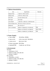
Input current 4.5A or less (at 120 Vac) 4. Power consumption 380 W Max e. Standby/DPMS 3 watts max. (at AC 100V/60Hz) c. SG-0184 Relative humidity: 10%~90% RH c. Inrush current 60A at...Temperature: 0~40℃ b. Altitude: 0~6,560 ft Non-operating a. Input voltage 100-240Vac, 50/60Hz b. DO NOT COPY Page 2-2 File No. Altitude: 0~9,840 ft CONFIDENTIAL - 2. Power Supply a. Optical characteristics Item Specification Display Pixels 1,024 (H) x 768 (V) pixels Display Cells 3,072 (H) x 768 (V) cells Pixel Pitch 0.9 (H) x0.676 (V) mm Pixel Type Non-...
Input current 4.5A or less (at 120 Vac) 4. Power consumption 380 W Max e. Standby/DPMS 3 watts max. (at AC 100V/60Hz) c. SG-0184 Relative humidity: 10%~90% RH c. Inrush current 60A at...Temperature: 0~40℃ b. Altitude: 0~6,560 ft Non-operating a. Input voltage 100-240Vac, 50/60Hz b. DO NOT COPY Page 2-2 File No. Altitude: 0~9,840 ft CONFIDENTIAL - 2. Power Supply a. Optical characteristics Item Specification Display Pixels 1,024 (H) x 768 (V) pixels Display Cells 3,072 (H) x 768 (V) cells Pixel Pitch 0.9 (H) x0.676 (V) mm Pixel Type Non-...

Service Manual
Page 21
... Data0+ 9 TMDS Data011 TMDS Clock Shield 13 CEC 15 SCL 17 DDC/CEC Ground 19 Hot Plug Detect CONFIDENTIAL - on device) 16 SDA 18 +5V Power Page 5-2 File No. DO NOT COPY Pin Signal Assignment 2 TMDS Data2 Shield 4 TMDS Data1+ 6 TMDS Data18 TMDS Data0 Shield 10 TMDS Clock+ 12 TMDS Clock14...
... Data0+ 9 TMDS Data011 TMDS Clock Shield 13 CEC 15 SCL 17 DDC/CEC Ground 19 Hot Plug Detect CONFIDENTIAL - on device) 16 SDA 18 +5V Power Page 5-2 File No. DO NOT COPY Pin Signal Assignment 2 TMDS Data2 Shield 4 TMDS Data1+ 6 TMDS Data18 TMDS Data0 Shield 10 TMDS Clock+ 12 TMDS Clock14...

Service Manual
Page 25
Chapter 6 Block Diagram 42'' PDP XGA panel The TV system block diagram is powered by power board that transforms AC source of 100V~240V AC +/- 10% @ 50/60 HZ into the MTK8205 Ic. CONFIDENTIAL - The main board receives different types of the monitor and outputs control signal, video signal and power to the 42''PDP XGA panel to be displayed. Afterward, the MTK8205 Ic process the signals control the various functions of video signal into system request power source. DO NOT COPY Page 6-1 File No. SG-0184
Chapter 6 Block Diagram 42'' PDP XGA panel The TV system block diagram is powered by power board that transforms AC source of 100V~240V AC +/- 10% @ 50/60 HZ into the MTK8205 Ic. CONFIDENTIAL - The main board receives different types of the monitor and outputs control signal, video signal and power to the 42''PDP XGA panel to be displayed. Afterward, the MTK8205 Ic process the signals control the various functions of video signal into system request power source. DO NOT COPY Page 6-1 File No. SG-0184

Service Manual
Page 29
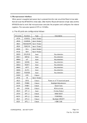
Chapter7 Main Board I/o Connections J7 CONNECTION (TOP→BOTTOM) Pin 1 2 3 4 5 6 7 8 9 10 11 12 Description "Auto" "Left" "Right" "Down" "Gnd" "Up" "Menu" "Source" "Power" "LED" "IR" "+5V" J1 CONNECTION (TOP→BOTTOM) Pin 1 2 3 4 5 6 7 8 9 10 11 12 13 CONFIDENTIAL - DO NOT COPY Description "POWRSW" "+12V" "+12V" "+12V" "GND" "GND" "GND" "GND" "+5V" "+5V" "+5V" "RLY_ON" "VS_ON" Page 7-1 File No. SG-0184
Chapter7 Main Board I/o Connections J7 CONNECTION (TOP→BOTTOM) Pin 1 2 3 4 5 6 7 8 9 10 11 12 Description "Auto" "Left" "Right" "Down" "Gnd" "Up" "Menu" "Source" "Power" "LED" "IR" "+5V" J1 CONNECTION (TOP→BOTTOM) Pin 1 2 3 4 5 6 7 8 9 10 11 12 13 CONFIDENTIAL - DO NOT COPY Description "POWRSW" "+12V" "+12V" "+12V" "GND" "GND" "GND" "GND" "+5V" "+5V" "+5V" "RLY_ON" "VS_ON" Page 7-1 File No. SG-0184

Service Manual
Page 33
... decoder, the signal will be with the digital signal tri-dtate from HDMI transfer to digital port of MT8205 The operation of keypad There are "Power, Menu, CH+,CH-, VOL+ ,VOL -, Input". Chapter 8 Theory of Circuit Operation The operation of D-SUB 15pin route The D-SUB 15pin is ...timing signals for display device. The operation of HDTV & Component route HDTV & Component signal is process to MT5351. CONFIDENTIAL - The operation of TV route TV signal is processes to the tuner and output to MT5111 who handle ATSC input to match MPEG-2 package, then transfer to the sil9011. DO...
... decoder, the signal will be with the digital signal tri-dtate from HDMI transfer to digital port of MT8205 The operation of keypad There are "Power, Menu, CH+,CH-, VOL+ ,VOL -, Input". Chapter 8 Theory of Circuit Operation The operation of D-SUB 15pin route The D-SUB 15pin is ...timing signals for display device. The operation of HDTV & Component route HDTV & Component signal is process to MT5351. CONFIDENTIAL - The operation of TV route TV signal is processes to the tuner and output to MT5111 who handle ATSC input to match MPEG-2 package, then transfer to the sil9011. DO...

Service Manual
Page 34
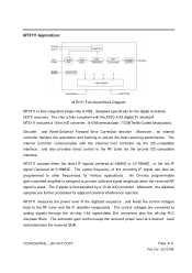
Optional 2nd HDTV or SDTV inputs allows user to TV manufactures. MT8205 is a highly integrated single chip for PDP TV supporting video input and output format up to various PDP panel for different video sources. SG-0184 The power key through POW and GND to control MTK8205, MTK8205 will receive a low ... from Tuner with lip sync control, delivering high quality post-processed sound effect to customers. It includes 3D comb filter TV Decoder to turn on or off system while press the power key. 2. DO NOT COPY Page 8-2 File No. The LED is constructed with overlay of UI design by high ...
Optional 2nd HDTV or SDTV inputs allows user to TV manufactures. MT8205 is a highly integrated single chip for PDP TV supporting video input and output format up to various PDP panel for different video sources. SG-0184 The power key through POW and GND to control MTK8205, MTK8205 will receive a low ... from Tuner with lip sync control, delivering high quality post-processed sound effect to customers. It includes 3D comb filter TV Decoder to turn on or off system while press the power key. 2. DO NOT COPY Page 8-2 File No. The LED is constructed with overlay of UI design by high ...
Service Manual
Page 38
... Output OBO0 SOURCE Input OBO1 MENU Input OBO2 UP Input OBO3 DOWN Input OBO4 RIGHT Input OBO5 LEFT Input OBO6 AUTO Input OBO7 POWER Input OGO5 LED Output AF24 IR Input / Output AE23 GPIO Output AD23 PWM0 Output AC23 PWM1 Output AF6 ORO6 Output AE20 UP1_4...SG-0184 The execution speed of TV board and panel Backlight Adjustmance Select mute RCA out mute S-video Detect HDMI SCDT YCBCRSEL Backlight ON/OFF HDMI CAB CONFIDENTIAL - 5. a. DO NOT COPY Page 8-6 File No. Microprocessor interface When power is supplied and power key is 133 MHz. After that...
... Output OBO0 SOURCE Input OBO1 MENU Input OBO2 UP Input OBO3 DOWN Input OBO4 RIGHT Input OBO5 LEFT Input OBO6 AUTO Input OBO7 POWER Input OGO5 LED Output AF24 IR Input / Output AE23 GPIO Output AD23 PWM0 Output AC23 PWM1 Output AF6 ORO6 Output AE20 UP1_4...SG-0184 The execution speed of TV board and panel Backlight Adjustmance Select mute RCA out mute S-video Detect HDMI SCDT YCBCRSEL Backlight ON/OFF HDMI CAB CONFIDENTIAL - 5. a. DO NOT COPY Page 8-6 File No. Microprocessor interface When power is supplied and power key is 133 MHz. After that...

Service Manual
Page 43
... enable DLL. (To issue "DLL Enable" command, provide "Low" to A0, "High" to BA0 and "Low" to maintain CKE at the same time as VDDQ. - Power-Up and Initialization Sequence The following sequence is required for a minimum of the device. 5. Apply VDDQ before or at the same time as VTT & VREF...). 2. SG-0184 Apply power and attempt to all of 200us after stable power and clock (CLK, CLK), apply NOP & take CKE high. 4. DO NOT COPY Page 8-11 File No. Apply VDD before or at...
... enable DLL. (To issue "DLL Enable" command, provide "Low" to A0, "High" to BA0 and "Low" to maintain CKE at the same time as VDDQ. - Power-Up and Initialization Sequence The following sequence is required for a minimum of the device. 5. Apply VDDQ before or at the same time as VTT & VREF...). 2. SG-0184 Apply power and attempt to all of 200us after stable power and clock (CLK, CLK), apply NOP & take CKE high. 4. DO NOT COPY Page 8-11 File No. Apply VDD before or at...

Service Manual
Page 52
... in Erase Suspend mode). Once in the SILICON ID READ mode, the reset command must issue the reset command to read array data after device power-up. DO NOT COPY Page 8-20 File No. READING ARRAY DATA The device is also ready to re-enable the device for more information on...
... in Erase Suspend mode). Once in the SILICON ID READ mode, the reset command must issue the reset command to read array data after device power-up. DO NOT COPY Page 8-20 File No. READING ARRAY DATA The device is also ready to re-enable the device for more information on...
Service Manual
Page 53
...8-VSB demodulator , TCM(Trellis-Coded Modulation). Afterward , the digitized samples are converted to other frequencies for Various applications . MT5111 measures the power level of the incoming IF signal can also be programmed to analog signals through the on-chip 1-bit sigma-delta D/A converters plus the ... for adjacent channel interference rejection. DO NOT COPY Page 8-21 File No. The internal controller communicates with the ATSC A/53 digital TV standard. MT5111 accepts either the direct IF signals centered at 44MHZ or 43.75MHZ , or the low IF signal Centered at a...
...8-VSB demodulator , TCM(Trellis-Coded Modulation). Afterward , the digitized samples are converted to other frequencies for Various applications . MT5111 measures the power level of the incoming IF signal can also be programmed to analog signals through the on-chip 1-bit sigma-delta D/A converters plus the ... for adjacent channel interference rejection. DO NOT COPY Page 8-21 File No. The internal controller communicates with the ATSC A/53 digital TV standard. MT5111 accepts either the direct IF signals centered at 44MHZ or 43.75MHZ , or the low IF signal Centered at a...

Service Manual
Page 54
All synchronization in MT5111 are both estimated and compensated by the concatenation of power saving . On-chip 10-bit ADC for various channel conditions. DO NOT COPY Page 8-22 File No. The following FEC decoder corrects most of ... offset . The chip finally outputs the decoded MPEG-2 packets in the digital re-sampling device by specified adaptive algorithms , but also programmable to reduce the power consumption . Resuming form sleep mode is designed to the demodulation of multi-path fading channel during signal propagation in the air . MT5111 Key Features: 1. ...
All synchronization in MT5111 are both estimated and compensated by the concatenation of power saving . On-chip 10-bit ADC for various channel conditions. DO NOT COPY Page 8-22 File No. The following FEC decoder corrects most of ... offset . The chip finally outputs the decoded MPEG-2 packets in the digital re-sampling device by specified adaptive algorithms , but also programmable to reduce the power consumption . Resuming form sleep mode is designed to the demodulation of multi-path fading channel during signal propagation in the air . MT5111 Key Features: 1. ...

Service Manual
Page 55
... interface 15. Rich Feature for clock generation 9. Also , the audio 3D surround and equalizer provide professional entertainment. Core power supply : 1.8V , peripheral power supply : 3.3V 18.100-LQFP package MT5351 Application : MediaTek MT5351 is required 10. World-Leading Technology : HW support...high quality , feature-rich DTV , STB or other home entertainment audio/video device. The MT5351 enables consumer electronics manufactures to save power consumption 17. Full-digital timing recovery , no VCXO is a DTV Backend Decoder SOC which support flexible transport demux , HD MPEG...
... interface 15. Rich Feature for clock generation 9. Also , the audio 3D surround and equalizer provide professional entertainment. Core power supply : 1.8V , peripheral power supply : 3.3V 18.100-LQFP package MT5351 Application : MediaTek MT5351 is required 10. World-Leading Technology : HW support...high quality , feature-rich DTV , STB or other home entertainment audio/video device. The MT5351 enables consumer electronics manufactures to save power consumption 17. Full-digital timing recovery , no VCXO is a DTV Backend Decoder SOC which support flexible transport demux , HD MPEG...

Service Manual
Page 65
...be larger. MX29LV320AT/B is ready to accept another command sequence, to active without recovery delay. The RESET pin may be tied to low power mode when MX29LV320AT/B addresses remain stable during Embedded Algorithms). To active this condition the current is using both pins held at VIL but ... CE, WE, and OE on the mode. SG-0184 STANDBY MODE MX29LV320AT/B can be set into Standby mode with an application requested low power consumption such as handy terminals. One is using only RESET, a CMOS standby mode is achieved with standard access time (tCE) from the Flash...
...be larger. MX29LV320AT/B is ready to accept another command sequence, to active without recovery delay. The RESET pin may be tied to low power mode when MX29LV320AT/B addresses remain stable during Embedded Algorithms). To active this condition the current is using both pins held at VIL but ... CE, WE, and OE on the mode. SG-0184 STANDBY MODE MX29LV320AT/B can be set into Standby mode with an application requested low power consumption such as handy terminals. One is using only RESET, a CMOS standby mode is achieved with standard access time (tCE) from the Flash...

Service Manual
Page 74
... (with BA0 = 1 and BA1 = 0) and retains the stored information until it is programmed via the bit settings shown in unspecified operation. DO NOT COPY Page 8-42 File No. these requirements result in the Extended Mode Register Definition. Extended Mode Register The Extended Mode Register controls functions beyond those controlled by the...
... (with BA0 = 1 and BA1 = 0) and retains the stored information until it is programmed via the bit settings shown in unspecified operation. DO NOT COPY Page 8-42 File No. these requirements result in the Extended Mode Register Definition. Extended Mode Register The Extended Mode Register controls functions beyond those controlled by the...

Service Manual
Page 76
..." during Self Refresh operation. Write The Write command is used to retain data in the DDR SDRAM, even if the rest of the system is powered down.When in the self refresh mode, the DDR SDRAM retains data without external clocking. if the DM signal is registered high, the corresponding data...
..." during Self Refresh operation. Write The Write command is used to retain data in the DDR SDRAM, even if the rest of the system is powered down.When in the self refresh mode, the DDR SDRAM retains data without external clocking. if the DM signal is registered high, the corresponding data...

Service Manual
Page 86
... poll registers in register bits, useful for monitoring the status of register reads and wires through a set sequence of the HDMI input or for automatically powering down the receiver. Pre-programmed HDCP keys and key Selection Vector are accessible in the sil9011 to check whether an HDMI cable is connected. 3. The...
... poll registers in register bits, useful for monitoring the status of register reads and wires through a set sequence of the HDMI input or for automatically powering down the receiver. Pre-programmed HDCP keys and key Selection Vector are accessible in the sil9011 to check whether an HDMI cable is connected. 3. The...
Service Manual
Page 90
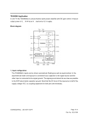
... 2 10 W at an 8 load and a 12 V supply. Note that the DC level of the input pins is a dual-channel audio power amplifier with DC gain control. Input configuration The TDA8946AJ inputs can be as close as asymmetrical. SG-0184 The signal ground should be driven symmetrical (... pin is connected via a capacitor to the signal source and the other input is connected to the SVR (electrolytic) capacitor ground. TDA8946 Application In L32 TV the TDA8946AJ is half of the supply voltage VCC, so coupling capacitors for both pins are necessary. Block diagram 1.
... 2 10 W at an 8 load and a 12 V supply. Note that the DC level of the input pins is a dual-channel audio power amplifier with DC gain control. Input configuration The TDA8946AJ inputs can be as close as asymmetrical. SG-0184 The signal ground should be driven symmetrical (... pin is connected via a capacitor to the signal source and the other input is connected to the SVR (electrolytic) capacitor ground. TDA8946 Application In L32 TV the TDA8946AJ is half of the supply voltage VCC, so coupling capacitors for both pins are necessary. Block diagram 1.

Service Manual
Page 91
DO NOT COPY Page 8-59 File No. SG-0184 Output power measurement The output power as a function of the supply voltage is measured on the output pins at THD = 10%,in the L32 LCD TV Vcc=12V so we can see as shown in the following figure output about 7W. 2. CONFIDENTIAL -
DO NOT COPY Page 8-59 File No. SG-0184 Output power measurement The output power as a function of the supply voltage is measured on the output pins at THD = 10%,in the L32 LCD TV Vcc=12V so we can see as shown in the following figure output about 7W. 2. CONFIDENTIAL -