Service Manual
Page 2
...DIAGRAM 134 6.1 GSM & UMTS RF Block 134 6.2 Interface Diagram 136 7. Circuit Diagram 143 8. DOWNLOAD 119 5.1 U250/KU250 DOWNLOAD 119 5.1.1 Introduction 119 5.1.2 Downloading Procedure 119 5.1.3 Troubleshooting Download Errors 129 5.1.4 Caution 133 6. WCDMA Test Mode ...Setting 154 10.2. PERFORMANCE 7 2.1 System Overview 7 2.2 Usable environment 8 2.3 Radio Performance 8 2.4 Current Consumption 14 2.5 RSSI BAR 14 2.6 Battery BAR 15 2.7 Sound Pressure Level 16 2.8 Charging 16 3. TECHNICAL BRIEF 17 3.1 General Description 17 3.2 GSM Mode 19 3.3 UMTS Mode 23...
...DIAGRAM 134 6.1 GSM & UMTS RF Block 134 6.2 Interface Diagram 136 7. Circuit Diagram 143 8. DOWNLOAD 119 5.1 U250/KU250 DOWNLOAD 119 5.1.1 Introduction 119 5.1.2 Downloading Procedure 119 5.1.3 Troubleshooting Download Errors 129 5.1.4 Caution 133 6. WCDMA Test Mode ...Setting 154 10.2. PERFORMANCE 7 2.1 System Overview 7 2.2 Usable environment 8 2.3 Radio Performance 8 2.4 Current Consumption 14 2.5 RSSI BAR 14 2.6 Battery BAR 15 2.7 Sound Pressure Level 16 2.8 Charging 16 3. TECHNICAL BRIEF 17 3.1 General Description 17 3.2 GSM Mode 19 3.3 UMTS Mode 23...
Service Manual
Page 6
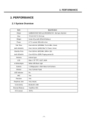
... External Memory I/O Connect Specification GSM900/1800/1900 and WCDMA2100 - PERFORMANCE 2.1 System Overview Item Shape Size Weight Power Talk Time (with 950mAh) Standby Time (with 950mAh Battery) 3.7 V normal, 950 mAh Li-Ion Over 200 min (WCDMA, Tx=12 dBm, Voice) Over 180 min (GSM, Max Tx Power, Voice) Over 350 Hrs (WCDMA...
... External Memory I/O Connect Specification GSM900/1800/1900 and WCDMA2100 - PERFORMANCE 2.1 System Overview Item Shape Size Weight Power Talk Time (with 950mAh) Standby Time (with 950mAh Battery) 3.7 V normal, 950 mAh Li-Ion Over 200 min (WCDMA, Tx=12 dBm, Voice) Over 180 min (GSM, Max Tx Power, Voice) Over 350 Hrs (WCDMA...

Service Manual
Page 14
2. PERFORMANCE 2.6 Battery BAR Indication Bar 4 Bar 4 → 3 Bar 3 → 2 Bar 2 → 1 Bar 1 → Empty Low Voltage, Warning message+ Blinking Power Off Standby Over 3.83 ± 0.05V 3.82 ± 0.05V 3.73 ± 0.05V 3.68 ± 0.05V 3.58 ± 0.05V 3.58± 0.05V (Stand-by) / 3.58 ± 0.05V (Talk) [Interval : 3min(Stand-by) / 1min(Talk)] 3.20 ± 0.05V - 15 -
2. PERFORMANCE 2.6 Battery BAR Indication Bar 4 Bar 4 → 3 Bar 3 → 2 Bar 2 → 1 Bar 1 → Empty Low Voltage, Warning message+ Blinking Power Off Standby Over 3.83 ± 0.05V 3.82 ± 0.05V 3.73 ± 0.05V 3.68 ± 0.05V 3.58 ± 0.05V 3.58± 0.05V (Stand-by) / 3.58 ± 0.05V (Talk) [Interval : 3min(Stand-by) / 1min(Talk)] 3.20 ± 0.05V - 15 -
Service Manual
Page 15
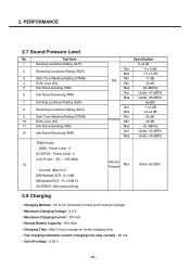
... -62 dBm 2.8 Charging • Charging Method : CC & CV (Constant Current and Constant Voltage) • Maximum Charging Voltage : 4.2 V • Maximum Charging Current : 700 mA • Normal Battery Capacity : 950 mAh • Charging Time : Max 3 hours (except for trickle charging time) • Full charging indication current (charging icon stop current) : 80 mA •...
... -62 dBm 2.8 Charging • Charging Method : CC & CV (Constant Current and Constant Voltage) • Maximum Charging Voltage : 4.2 V • Maximum Charging Current : 700 mA • Normal Battery Capacity : 950 mAh • Charging Time : Max 3 hours (except for trickle charging time) • Full charging indication current (charging icon stop current) : 80 mA •...
Service Manual
Page 17
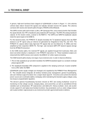
...stage of power amplifier from RF-to baseband in the RTR6275 transceiver IC. It monitors and controls the external power source and coordinates battery recharging while maintaining the handset supply voltages using an internal LO generated by integrated on-chip PLL and VCO. Various oscillator, clock,... amplitude-modulated (AM) component is shown in order to the MSM IC. TECHNICAL BRIEF A generic, high-level functional block diagram of U250/KU250 is applied to the ramping control pin of up -converter translates the GMSK-modulated signal to the MSM IC. 3. For the transmit chains,...
...stage of power amplifier from RF-to baseband in the RTR6275 transceiver IC. It monitors and controls the external power source and coordinates battery recharging while maintaining the handset supply voltages using an internal LO generated by integrated on-chip PLL and VCO. Various oscillator, clock,... amplitude-modulated (AM) component is shown in order to the MSM IC. TECHNICAL BRIEF A generic, high-level functional block diagram of U250/KU250 is applied to the ramping control pin of up -converter translates the GMSK-modulated signal to the MSM IC. 3. For the transmit chains,...
Service Manual
Page 26
...for over-current protection - Eleven low dropout regulator circuits with programmable thresholds - TCXO buffer control for power savings - Battery voltage detectors with programmable output voltages, implemented using three different current ratings: 300 mA (two), 150 mA (six...Analog multiplexer selects from 8 internal and up and synchronize, deglitch, and buffer the TCXO signal - Supports lithium-ion main batteries - Crystal oscillator detector and automated switch-over -temperature protection (smart thermal control) - 27 - Valid external supply attachment and...
...for over-current protection - Eleven low dropout regulator circuits with programmable thresholds - TCXO buffer control for power savings - Battery voltage detectors with programmable output voltages, implemented using three different current ratings: 300 mA (two), 150 mA (six...Analog multiplexer selects from 8 internal and up and synchronize, deglitch, and buffer the TCXO signal - Supports lithium-ion main batteries - Crystal oscillator detector and automated switch-over -temperature protection (smart thermal control) - 27 - Valid external supply attachment and...
Service Manual
Page 44
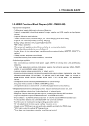
PM6650 cover the power of MSM6245, MSM memory, RF block, Bluetooth, USIM and TCXO. battery, external charger, adapter, coin cell back-up and signal buffering, and key parameters (under-voltage lockout and crystal oscillator signal ...power-on sequence. - 45 - and generates all wireless handset power management. Eight programmable output voltages are within acceptable operational limits, and coordinates battery and coin cell recharging while maintaining the handset electronics supply voltages. TECHNICAL BRIEF 3.9 Power Block 3.9.1. The power management portion accepts power from ...
PM6650 cover the power of MSM6245, MSM memory, RF block, Bluetooth, USIM and TCXO. battery, external charger, adapter, coin cell back-up and signal buffering, and key parameters (under-voltage lockout and crystal oscillator signal ...power-on sequence. - 45 - and generates all wireless handset power management. Eight programmable output voltages are within acceptable operational limits, and coordinates battery and coin cell recharging while maintaining the handset electronics supply voltages. TECHNICAL BRIEF 3.9 Power Block 3.9.1. The power management portion accepts power from ...

Service Manual
Page 46
...2V~3.82V 100~70 (%) 3.81V~3.74V 69~45 (%) 3.73V~3.69V 44~20 (%) 3.68V~3.59V 19~3 (%) 3.58V~3.20V 2~0 (%) Figure 1.13 U250/KU250 Battery Bar Display(Stand By Condition) - 47 - These pins are connected to pin (VCHG). It is used and when to capture variations over time, this pin... (VCHG) is monitored by detection circuitry to ascertain whether a valid external supply is routed internally to set limits for battery charging. PM6650 circuits monitor voltages at VCHARGER and ICHARGE pins to determine which supply should be used for the charging current. 3. The...
...2V~3.82V 100~70 (%) 3.81V~3.74V 69~45 (%) 3.73V~3.69V 44~20 (%) 3.68V~3.59V 19~3 (%) 3.58V~3.20V 2~0 (%) Figure 1.13 U250/KU250 Battery Bar Display(Stand By Condition) - 47 - These pins are connected to pin (VCHG). It is used and when to capture variations over time, this pin... (VCHG) is monitored by detection circuitry to ascertain whether a valid external supply is routed internally to set limits for battery charging. PM6650 circuits monitor voltages at VCHARGER and ICHARGE pins to determine which supply should be used for the charging current. 3. The...

Service Manual
Page 47
Parameter Min Typ Max Unit Trickle Current 60 80 100 mA - 48 - The charging current is on-chip programmable current source that supplies current from VDD to 80mA. TECHNICAL BRIEF Trickle Charging Trickle Charging of the main battery, enabled through SBI control and powered from VDD, is provided by the PM6650 IC, The trickle charger is set to pin (VBAT). Trickle charging can be used for lithium-ion and nickelbased batteries, with its performance specified below (3.2V). 3.
Parameter Min Typ Max Unit Trickle Current 60 80 100 mA - 48 - The charging current is on-chip programmable current source that supplies current from VDD to 80mA. TECHNICAL BRIEF Trickle Charging Trickle Charging of the main battery, enabled through SBI control and powered from VDD, is provided by the PM6650 IC, The trickle charger is set to pin (VBAT). Trickle charging can be used for lithium-ion and nickelbased batteries, with its performance specified below (3.2V). 3.

Service Manual
Page 48
... Method : CC & CV (Constant Current & Constant Voltage) • Maximum Charging Voltage : 4.2V • Maximum Charging Current : 600mA • Nominal Battery Capacity : 950mAh • Charger Voltage : 5.1V • Charging time : Max 3h (Except time trickle charging) • Full charge indication current (icon... stop current) : 100mA • Low battery POP UP : Idle - 3.58V, Dedicated(GSM/WCDMA) - 3.58V • Low battery alarm interval : Idle - 3 min, Dedicated - 1min • Cut-off voltage : 3.20V - 49 - ...
... Method : CC & CV (Constant Current & Constant Voltage) • Maximum Charging Voltage : 4.2V • Maximum Charging Current : 600mA • Nominal Battery Capacity : 950mAh • Charger Voltage : 5.1V • Charging time : Max 3h (Except time trickle charging) • Full charge indication current (icon... stop current) : 100mA • Low battery POP UP : Idle - 3.58V, Dedicated(GSM/WCDMA) - 3.58V • Low battery alarm interval : Idle - 3 min, Dedicated - 1min • Cut-off voltage : 3.20V - 49 - ...

Service Manual
Page 55
....3 HKADC(House Keeping ADC) The MSM6245 device has an on-chip 8-bit analog-to-digital converter (HKADC) which are multiplexed to analog parameters such as battery voltage, temperature, and RF power levels. The MSM6245 device has six analog input pins which is tended to digitize DC signals corresponding to the input... - 3. Channel HKADC0 HKADC1 HKADC2 HKADC3 HKADC4 HKADC5 Figure 1.18 MSM6245 HKADC Block diagram Signal AMUX_OUT VBATT_SENSE NC NC PCB_Rev_ADC Battery_THERM Note RF PAM Temperature Check Battery voltage level NC NC PCB Version Check...
....3 HKADC(House Keeping ADC) The MSM6245 device has an on-chip 8-bit analog-to-digital converter (HKADC) which are multiplexed to analog parameters such as battery voltage, temperature, and RF power levels. The MSM6245 device has six analog input pins which is tended to digitize DC signals corresponding to the input... - 3. Channel HKADC0 HKADC1 HKADC2 HKADC3 HKADC4 HKADC5 Figure 1.18 MSM6245 HKADC Block diagram Signal AMUX_OUT VBATT_SENSE NC NC PCB_Rev_ADC Battery_THERM Note RF PAM Temperature Check Battery voltage level NC NC PCB Version Check...

Service Manual
Page 70
Connector - 71 - TECHNICAL BRIEF Logic / Audio BAT300 U303 CN403 CN401 U402 Reference BAT300 U303 U402 Description Backup Battery 1.3M Cam. LDO Audio AMP Reference CN401 CN403 Description MMI connector (18pin) 1.3M Cam. 3.
Connector - 71 - TECHNICAL BRIEF Logic / Audio BAT300 U303 CN403 CN401 U402 Reference BAT300 U303 U402 Description Backup Battery 1.3M Cam. LDO Audio AMP Reference CN401 CN403 Description MMI connector (18pin) 1.3M Cam. 3.
Service Manual
Page 93
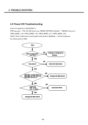
YES Key press? NO Change or charging the Battery NO Check the Key Dome YES VREG_MSMC_1.2V,VREG_MSMP_2.7V, VREG_MSME_1.8V, VREG_TCXO_2.85V, VREG_MSMA_2.6V power up and system reset assert to MSM6245 → ... : 19.2M X300 : 32.768Khz YES Change the Main board NO Check the TXCO - 94 - 4. TROUBLE SHOOTING 4.9 Power ON Troubleshooting Power On sequence of U250/KU250 is : PWR key press → PM_ON_SW_N go to PMIC Start...
YES Key press? NO Change or charging the Battery NO Check the Key Dome YES VREG_MSMC_1.2V,VREG_MSMP_2.7V, VREG_MSME_1.8V, VREG_TCXO_2.85V, VREG_MSMA_2.6V power up and system reset assert to MSM6245 → ... : 19.2M X300 : 32.768Khz YES Change the Main board NO Check the TXCO - 94 - 4. TROUBLE SHOOTING 4.9 Power ON Troubleshooting Power On sequence of U250/KU250 is : PWR key press → PM_ON_SW_N go to PMIC Start...
Service Manual
Page 95
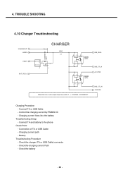
... TA or USB Cable - Check the charger (TA or USB Cable) connector - Charging current flows into the battery Troubleshooting Setup - Connect TA and battery to the phone Check Point - Connection of TA or USB Cable - Battery Troubleshooting Procedure - Control the charging current by PM6650 IC - Check the charging current Path - TROUBLE SHOOTING 4.10...
... TA or USB Cable - Check the charger (TA or USB Cable) connector - Charging current flows into the battery Troubleshooting Setup - Connect TA and battery to the phone Check Point - Connection of TA or USB Cable - Battery Troubleshooting Procedure - Control the charging current by PM6650 IC - Check the charging current Path - TROUBLE SHOOTING 4.10...
Service Manual
Page 96
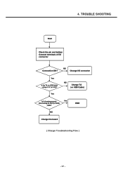
END NO Change the board [ Charger Troubleshooting Flow ] - 97 - Yes NO Change TA (or USB Cable) Is it charging properly Yes After turning on Q301(or Q302) , Q302? NO Change I /O connector Connection OK? 4. TROUBLE SHOOTING Start Check the pin and battery Connect terminals of I /O connector Yes Is the TA (or USB Cable) voltage 5.1V (or 5.0V)?
END NO Change the board [ Charger Troubleshooting Flow ] - 97 - Yes NO Change TA (or USB Cable) Is it charging properly Yes After turning on Q301(or Q302) , Q302? NO Change I /O connector Connection OK? 4. TROUBLE SHOOTING Start Check the pin and battery Connect terminals of I /O connector Yes Is the TA (or USB Cable) voltage 5.1V (or 5.0V)?

Service Manual
Page 104
Yes Backlight LED ON? 4. No Change the Main board NO NO YES Check battery Yes Change the Main board END +VPWR KEY_BACK_LIGHT LED(8EA) +VPWR LD400 LEBB-S14H LD403 LEBB-S14H LD406 LEBB-S14H REV_B : EDLH0013501 --> EDLH0006001 R411 100ohm ...
Yes Backlight LED ON? 4. No Change the Main board NO NO YES Check battery Yes Change the Main board END +VPWR KEY_BACK_LIGHT LED(8EA) +VPWR LD400 LEBB-S14H LD403 LEBB-S14H LD406 LEBB-S14H REV_B : EDLH0013501 --> EDLH0006001 R411 100ohm ...

Service Manual
Page 158
Description IMT,BAR/FLIP 2 AAAY00 ADDITION 3 MCJA00 COVER,BATTERY 2 APAY00 PACKAGE 3 BSEA00 SUPPLEMENTARY PART 2 APEY00 PHONE 3 ACGK00 COVER ASSY,FRONT 4 MCCC00 CAP,EARPHONE JACK 4 MCCG00 CAP,MULTIMEDIA CARD 4 MCJK00 COVER,FRONT 5 MICE00 INSERT,NUT 5 ...
Description IMT,BAR/FLIP 2 AAAY00 ADDITION 3 MCJA00 COVER,BATTERY 2 APAY00 PACKAGE 3 BSEA00 SUPPLEMENTARY PART 2 APEY00 PHONE 3 ACGK00 COVER ASSY,FRONT 4 MCCC00 CAP,EARPHONE JACK 4 MCCG00 CAP,MULTIMEDIA CARD 4 MCJK00 COVER,FRONT 5 MICE00 INSERT,NUT 5 ...

Service Manual
Page 160
...:60% 4 SAFF00 PCB ASSY,MAIN,SMT SAFF0117802 5 SAFC00 PCB ASSY,MAIN,SMT BOTTOM SAFC0088501 6 ANT103 ANTENNA,GSM,FIXED SNGF0026001 3.0 ,-2.0 dBd, ,Bluetooth, SMD, 8.0*2.0*1.2 ,; ,SINGLE ,2.0 ,50 ,3.0 6 BAT300 BATTERY,CELL,LITHIUM SBCL0001701 2 V,0.5 mAh,CYLINDER ,Reflow type BB, Max T 1.67, phi 4.8, Pb-Free 6 C101 CAP,CHIP,MAKER ECZH0000841 56 pF,50V ,J ,NP0 ,TC ,1005 ,R/TP...
...:60% 4 SAFF00 PCB ASSY,MAIN,SMT SAFF0117802 5 SAFC00 PCB ASSY,MAIN,SMT BOTTOM SAFC0088501 6 ANT103 ANTENNA,GSM,FIXED SNGF0026001 3.0 ,-2.0 dBd, ,Bluetooth, SMD, 8.0*2.0*1.2 ,; ,SINGLE ,2.0 ,50 ,3.0 6 BAT300 BATTERY,CELL,LITHIUM SBCL0001701 2 V,0.5 mAh,CYLINDER ,Reflow type BB, Max T 1.67, phi 4.8, Pb-Free 6 C101 CAP,CHIP,MAKER ECZH0000841 56 pF,50V ,J ,NP0 ,TC ,1005 ,R/TP...
Service Manual
Page 173
...-240V ,5060 Hz,5.1 V,.7 A,CE ,AC-DC ADAPTOR ,; ,85Vac~264Vac ,5.1V(+0.15V, -0.2V) ,700mA ,5060 , ,WALL 2P ,I/O CONNECTOR , Color Black Remark 35 - 174 - 11. Description 3 SBPL00 BATTERY PACK,LI-ION 3 SSAD00 ADAPTOR,AC-DC ADAPTOR,AC-DC ADAPTOR,AC-DC ADAPTOR,AC-DC Part Number Spec 3.7 V,950 mAh,1 CELL,PRISMATIC...
...-240V ,5060 Hz,5.1 V,.7 A,CE ,AC-DC ADAPTOR ,; ,85Vac~264Vac ,5.1V(+0.15V, -0.2V) ,700mA ,5060 , ,WALL 2P ,I/O CONNECTOR , Color Black Remark 35 - 174 - 11. Description 3 SBPL00 BATTERY PACK,LI-ION 3 SSAD00 ADAPTOR,AC-DC ADAPTOR,AC-DC ADAPTOR,AC-DC ADAPTOR,AC-DC Part Number Spec 3.7 V,950 mAh,1 CELL,PRISMATIC...

