User's Guide
Page 11
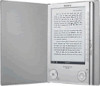
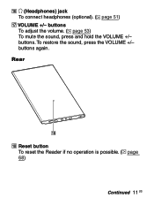
buttons To adjust the volume. ( page 53) To mute the sound, press and hold the VOLUME +/- buttons again. To restore the sound, press the VOLUME +/- (Headphones) jack To connect headphones (optional). ( page 51) VOLUME +/- Rear Reset button To reset the Reader if no operation is possible. ( page 68) Continued 11 US buttons.
buttons To adjust the volume. ( page 53) To mute the sound, press and hold the VOLUME +/- buttons again. To restore the sound, press the VOLUME +/- (Headphones) jack To connect headphones (optional). ( page 51) VOLUME +/- Rear Reset button To reset the Reader if no operation is possible. ( page 68) Continued 11 US buttons.
User's Guide
Page 15
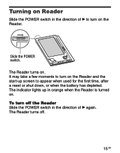
Slide the POWER switch. The Reader turns on the Reader and the start-up in the direction of to turn on . To turn on . The Reader turns off the Reader Slide the POWER switch in orange when the Reader is turned on the Reader. The indicator lights up screen to appear when used for the first time, after a reset or shut down, or when the battery has depleted. It may take a few moments to turn off . 15 US Turning on Reader Slide the POWER switch in the direction of again.
Slide the POWER switch. The Reader turns on the Reader and the start-up in the direction of to turn on . To turn on . The Reader turns off the Reader Slide the POWER switch in orange when the Reader is turned on the Reader. The indicator lights up screen to appear when used for the first time, after a reset or shut down, or when the battery has depleted. It may take a few moments to turn off . 15 US Turning on Reader Slide the POWER switch in the direction of again.
User's Guide
Page 68
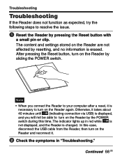
... reconnect it. Check the symptoms in red while is not displayed, and the Reader is displayed, and you connect the Reader to resolve the issue. Reset the Reader by sliding the POWER switch. The indicator lights up in "Troubleshooting." In this time. Note • When ...you will not be able to turn on the Reader again. Continued 68 US Otherwise, it is erased. Troubleshooting Troubleshooting If the Reader does not function as expected, try the following steps to your computer after a reset, it takes about 40 minutes until (indicating connection via USB...
... reconnect it. Check the symptoms in red while is not displayed, and the Reader is displayed, and you connect the Reader to resolve the issue. Reset the Reader by sliding the POWER switch. The indicator lights up in "Troubleshooting." In this time. Note • When ...you will not be able to turn on the Reader again. Continued 68 US Otherwise, it is erased. Troubleshooting Troubleshooting If the Reader does not function as expected, try the following steps to your computer after a reset, it takes about 40 minutes until (indicating connection via USB...
User's Guide
Page 95
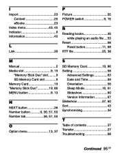
... eBooks 23 Index menu 43, 45 Indicator 9 Information 42 L Link 39 P Picture 55 POWER switch 9, 15 R Reading books 35 while playing an audio file.....53 Reset 68 Reset button 11, 68 RTF file 25, 38 M Manual 2 Media slot 9, 19 "Memory Stick Duo" slot.........9 SD Memory Card slot 9 Memory Card 19 "Memory Stick...
... eBooks 23 Index menu 43, 45 Indicator 9 Information 42 L Link 39 P Picture 55 POWER switch 9, 15 R Reading books 35 while playing an audio file.....53 Reset 68 Reset button 11, 68 RTF file 25, 38 M Manual 2 Media slot 9, 19 "Memory Stick Duo" slot.........9 SD Memory Card slot 9 Memory Card 19 "Memory Stick...

Service Manual
Page 5
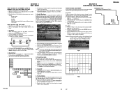
.... MENU button To return to Parts and Controls Holes for soft cover attachment The soft cover is extracted from instruction manual. SECTION 2 GENERAL PRS-505 This section is attached when purchased. Folds open in use 1 2 3 4 5 6 7 8 9 0 Front Enter button*1 To decide an item or apply a setting, press the Enter button...
.... MENU button To return to Parts and Controls Holes for soft cover attachment The soft cover is extracted from instruction manual. SECTION 2 GENERAL PRS-505 This section is attached when purchased. Folds open in use 1 2 3 4 5 6 7 8 9 0 Front Enter button*1 To decide an item or apply a setting, press the Enter button...
Service Manual
Page 11
... card or memory stick. 3. TER] button or the [0] button. 2. Download the as follow as "/Sony Reader/software" on the flexible board. The file of the LUT is -1.16 V.) Fig. ... state of a Power Off tab of LUT (Look Up Table) and rewrite. PRS-505 11 SECTION 5 ELECTRICAL ADJUSTMENT PRS-505 VCOM VOLTAGE ADJUSTMENT Vcom voltage for the display panel varies for the SD memory card... In the state that the slideshow starts. 3. Power Off 1. It's back to directly. Reset Screen Lock The screen lock can be performed while changing the screen. Specify a desired screen, ...
... card or memory stick. 3. TER] button or the [0] button. 2. Download the as follow as "/Sony Reader/software" on the flexible board. The file of the LUT is -1.16 V.) Fig. ... state of a Power Off tab of LUT (Look Up Table) and rewrite. PRS-505 11 SECTION 5 ELECTRICAL ADJUSTMENT PRS-505 VCOM VOLTAGE ADJUSTMENT Vcom voltage for the display panel varies for the SD memory card... In the state that the slideshow starts. 3. Power Off 1. It's back to directly. Reset Screen Lock The screen lock can be performed while changing the screen. Specify a desired screen, ...
Service Manual
Page 12
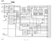
...CLK CKE RAS CAS CS WE D0 - A19 NOR FLASH MEMORY IC1203 CE 26 WE 11 OE 28 RY/BY 15 RESET 12 BD0 - BD15 BA1 - BA7 BA8 - BD15 ADDRESS DECODER IC203 BA21 - D7 D8 - A10, A12 -... DUO/ SD MEMORY CARD XCS H2 XRESET D1 BD0 - A23 BD0 - D31 A2 - A23 A1 - BA20 DQ0 - I /01 - PRS-505 SECTION 6 DIAGRAMS 6-1. BA15 BA1 - BD15 BA1 - BD15 IC1107 (2/2) DQM2 DQM3 MA10 MA11 SDCLK SDCKEO #RAS #CAS #CS2 #SDWE 15 39...ALE E10 NAND-CLE A10 NAND-CE0 B9 RY/#BY A7 USB20INT KA134 XRESET-OUT A3 VBUS PRS-505 12 12 BA23 BA1 BD0 - A8, A11, A12, BA0, BA1 SD-RAM IC1201 BD0 - MAIN Section (1/2) ...
...CLK CKE RAS CAS CS WE D0 - A19 NOR FLASH MEMORY IC1203 CE 26 WE 11 OE 28 RY/BY 15 RESET 12 BD0 - BD15 BA1 - BA7 BA8 - BD15 ADDRESS DECODER IC203 BA21 - D7 D8 - A10, A12 -... DUO/ SD MEMORY CARD XCS H2 XRESET D1 BD0 - A23 BD0 - D31 A2 - A23 A1 - BA20 DQ0 - I /01 - PRS-505 SECTION 6 DIAGRAMS 6-1. BA15 BA1 - BD15 BA1 - BD15 IC1107 (2/2) DQM2 DQM3 MA10 MA11 SDCLK SDCKEO #RAS #CAS #CS2 #SDWE 15 39...ALE E10 NAND-CLE A10 NAND-CE0 B9 RY/#BY A7 USB20INT KA134 XRESET-OUT A3 VBUS PRS-505 12 12 BA23 BA1 BD0 - A8, A11, A12, BA0, BA1 SD-RAM IC1201 BD0 - MAIN Section (1/2) ...

Service Manual
Page 14
...SHDN 4 + CURRENT DETECT IC1803 Q472 VOLTAGE DETECTOR IC408 BATTERY CONTROL SWITCH Q801, 802 B+ SWITCH Q402, 405, 406 BUFFER Q403 RESET IC407 5Q CK 1 6 CLR PR 7 Q401 VOLTAGE DETECTOR IC404 V2 VCORE V3 +2.9V REGULATOR IC402 +1.9V REGULATOR IC403 +3.1V REGULATOR IC409 1 LDO 12 TS ... BAT 5, 6 AC 4 S801 RESET VOLTAGE DETECTOR IC802 +2.9V REGULATOR IC406 V1 VOLTAGE DETECTOR IC405 D1805 PS401 8PWR_POS 8PWR_GATE 8PWR_NEG, 8PWR_POS, 8PWR_GATA C (Page 13) 8PWR_NEG VBUS A (Page 12) LITHIUM ION BATTERY 3.7V 600mAh J001 - + DC IN 5.2V PRS-505 14 14 KSI7 FROM POWER SWITCH ...
...SHDN 4 + CURRENT DETECT IC1803 Q472 VOLTAGE DETECTOR IC408 BATTERY CONTROL SWITCH Q801, 802 B+ SWITCH Q402, 405, 406 BUFFER Q403 RESET IC407 5Q CK 1 6 CLR PR 7 Q401 VOLTAGE DETECTOR IC404 V2 VCORE V3 +2.9V REGULATOR IC402 +1.9V REGULATOR IC403 +3.1V REGULATOR IC409 1 LDO 12 TS ... BAT 5, 6 AC 4 S801 RESET VOLTAGE DETECTOR IC802 +2.9V REGULATOR IC406 V1 VOLTAGE DETECTOR IC405 D1805 PS401 8PWR_POS 8PWR_GATE 8PWR_NEG, 8PWR_POS, 8PWR_GATA C (Page 13) 8PWR_NEG VBUS A (Page 12) LITHIUM ION BATTERY 3.7V 600mAh J001 - + DC IN 5.2V PRS-505 14 14 KSI7 FROM POWER SWITCH ...

Service Manual
Page 16
PRS-505 PRS-505 6-4. C E C Q104 B R101 R104 PS401 C1206 C955 L953 IC1203 L1101 L1201 TP830 C1101 C1219 C1218 TP829 CN801 12 1 R842 TP802 R836 R821 48 RB806 RB805 RB801 ... C406 IC401 R423 A D403 K A 9 10 11 12 R403 R421 R402 1 5 C407 IC402 3 4 R409 R407 R406 R404 R405 C405 C413 R427 R428 R429 R430 R425 R431 RESET C408 C403 C426 C425 4 3 5 Q402 2 6 1 R426 R424 321 C Q406 Q405 456 B E K D402 A C404 THP401 L402 I1C4035 3 4 R411 C416 C417 16 C1108 L403 1 C1016 C1018 L1004...
PRS-505 PRS-505 6-4. C E C Q104 B R101 R104 PS401 C1206 C955 L953 IC1203 L1101 L1201 TP830 C1101 C1219 C1218 TP829 CN801 12 1 R842 TP802 R836 R821 48 RB806 RB805 RB801 ... C406 IC401 R423 A D403 K A 9 10 11 12 R403 R421 R402 1 5 C407 IC402 3 4 R409 R407 R406 R404 R405 C405 C413 R427 R428 R429 R430 R425 R431 RESET C408 C403 C426 C425 4 3 5 Q402 2 6 1 R426 R424 321 C Q406 Q405 456 B E K D402 A C404 THP401 L402 I1C4035 3 4 R411 C416 C417 16 C1108 L403 1 C1016 C1018 L1004...

Service Manual
Page 21
...SDDO4 SDDO5 SDDO6 VCC GND VCCI SDDO7 SDCLK SDOE GDOE GDSP GDCLK GND TCK TDI TMS VMV VMV GND RESERVED ERR STBY RDY RESET PDOE RESERVED RESERVED RESERVED VCC GND VCCIB TEST1 TEST0 TEST2 RESERVED PWR3 I2CSDA I2CSCL SPICS SPIDI SPICLK SPIDO TP301 TP302 TP303 TP304 TP305... 8-25V 8-COMMON 8-5V (Page 20) 8BORDER0 8BORDER1 8PWR_GATE 8COM_CTRL 8PWR_POS 8PWR_NEG 8BORDER0 8BORDER1 8PWR_GATE 8COM_CTRL (Page 20) 8PWR_POS 8PWR_NEG GND (Page 20) PRS-505 21 21 Note: When IC301 on the MAIN board is damaged, exchange the new MAIN board for IC Pin Function Description. SCHEMATIC DIAGRAM - 6-9.
...SDDO4 SDDO5 SDDO6 VCC GND VCCI SDDO7 SDCLK SDOE GDOE GDSP GDCLK GND TCK TDI TMS VMV VMV GND RESERVED ERR STBY RDY RESET PDOE RESERVED RESERVED RESERVED VCC GND VCCIB TEST1 TEST0 TEST2 RESERVED PWR3 I2CSDA I2CSCL SPICS SPIDI SPICLK SPIDO TP301 TP302 TP303 TP304 TP305... 8-25V 8-COMMON 8-5V (Page 20) 8BORDER0 8BORDER1 8PWR_GATE 8COM_CTRL 8PWR_POS 8PWR_NEG 8BORDER0 8BORDER1 8PWR_GATE 8COM_CTRL (Page 20) 8PWR_POS 8PWR_NEG GND (Page 20) PRS-505 21 21 Note: When IC301 on the MAIN board is damaged, exchange the new MAIN board for IC Pin Function Description. SCHEMATIC DIAGRAM - 6-9.

Service Manual
Page 23
... (Page 19) SRDSP STCK STFS STXD USB20INT (Page 22) (Page 18) PCSDCARD PCMSCARD SDWP SDDET PCR5CCLK VBUS (Page 22) LED2-ORG (Page 24) PRS-505 A(24-0) D(31-0) (Page 25) (Page 27) V2 GND GND VCORE R2010 680 RB2011 330 RXD TXD RTS CTS C1029 0.1 TP1589 RB2012 330 TP1588 ...R2267 100k TP2005 TRST C1019 0.1 TP2007 BOOT0 R2214 10k R2215 10k R2119 10k TP2008 BOOT2 TP2006 BOOT1 R2264 100k C1031 0.1 C1032 0.01 C1033 0.1 TP1025 RESET-SF TP1024 SDCKE1 C1016 R2268 0.1 100k C1015 0.1 C1017 0.1 C1018 10 L1004 47μH TP1022 PA18 TP1023 PA20 C1014 0.1 C1013 0.1 RB2007 100 ...
... (Page 19) SRDSP STCK STFS STXD USB20INT (Page 22) (Page 18) PCSDCARD PCMSCARD SDWP SDDET PCR5CCLK VBUS (Page 22) LED2-ORG (Page 24) PRS-505 A(24-0) D(31-0) (Page 25) (Page 27) V2 GND GND VCORE R2010 680 RB2011 330 RXD TXD RTS CTS C1029 0.1 TP1589 RB2012 330 TP1588 ...R2267 100k TP2005 TRST C1019 0.1 TP2007 BOOT0 R2214 10k R2215 10k R2119 10k TP2008 BOOT2 TP2006 BOOT1 R2264 100k C1031 0.1 C1032 0.01 C1033 0.1 TP1025 RESET-SF TP1024 SDCKE1 C1016 R2268 0.1 100k C1015 0.1 C1017 0.1 C1018 10 L1004 47μH TP1022 PA18 TP1023 PA20 C1014 0.1 C1013 0.1 RB2007 100 ...

Service Manual
Page 24
... XC61CN2502NR C807 8p C808 8p C803 0.01 R851 1k R833 1M X802 4.9152MHz R819 R837 470k 470k R808 470k S801 RESET C806 0.1 TP1516 TP1517 TP1518 TP1519 TP1520 TP1521 TP1522 TP1523 PRS-505 24 24 PRS-505 6-12. MAIN Board (7/10) - • See page 15 for waveform. • See page 34 for IC Pin Function Description...
... XC61CN2502NR C807 8p C808 8p C803 0.01 R851 1k R833 1M X802 4.9152MHz R819 R837 470k 470k R808 470k S801 RESET C806 0.1 TP1516 TP1517 TP1518 TP1519 TP1520 TP1521 TP1522 TP1523 PRS-505 24 24 PRS-505 6-12. MAIN Board (7/10) - • See page 15 for waveform. • See page 34 for IC Pin Function Description...

Service Manual
Page 27
...Board (10/10) - • See page 29 for IC Block Diagram. • See page 34 for IC Pin Function Description. SCHEMATIC DIAGRAM - PRS-505 (10/10) (Page 24) STAT1 USB_VBUS DC+ DC- (Page 22) TP402 DC TP400 GND TP403 DC D420 CRS01(TE85R) PS401 2A 32V D401 DAN222... R417 470k Q401 2SC4738F-Y/GR INVERTER C422 0.1 RESET IC407 TC7WH74FK Q CK D C430 1 GND Q R418 4.7k R477 470k C423 0.1 R419 100k R420 470k Q403 2SA1832F-GR BUFFER Q472 SSM3K03FE(TPL3) INVERTER R475 22k S C449 0.1 C427 0.1 V1 (Page 24) RESET LOW-BATT-LI BATT-LI (Page 24) V3 (Page 22) PRS-505 27 27 6-15.
...Board (10/10) - • See page 29 for IC Block Diagram. • See page 34 for IC Pin Function Description. SCHEMATIC DIAGRAM - PRS-505 (10/10) (Page 24) STAT1 USB_VBUS DC+ DC- (Page 22) TP402 DC TP400 GND TP403 DC D420 CRS01(TE85R) PS401 2A 32V D401 DAN222... R417 470k Q401 2SC4738F-Y/GR INVERTER C422 0.1 RESET IC407 TC7WH74FK Q CK D C430 1 GND Q R418 4.7k R477 470k C423 0.1 R419 100k R420 470k Q403 2SA1832F-GR BUFFER Q472 SSM3K03FE(TPL3) INVERTER R475 22k S C449 0.1 C427 0.1 V1 (Page 24) RESET LOW-BATT-LI BATT-LI (Page 24) V3 (Page 22) PRS-505 27 27 6-15.
Service Manual
Page 34
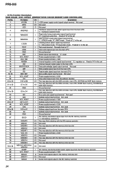
... memory 31 to 33 D7 to D5 I/O Two-way data bus with the memory stick duo slot 78 to 84 MDIO15, MDIO19 to D4 I Reset signal input terminal "L": reset 12 VCC_ROUT - Power supply terminal (+3.3V) 74 MDIO13 I/O Not used 75 MSDAT2 I/O Two-way data bus with the memory stick duo slot 76... mode, "H": WAIT mode Fixed at "L" in this set 15 INT O Interrupt request signal output to A17 I Byte enable signal input terminal Not used 42 VCC_ROUT - PRS-505 • IC Pin Function Description MAIN BOARD IC201 R5C807 (MEMORY STICK DUO/SD MEMORY CARD CONTROLLER) Pin No.
... memory 31 to 33 D7 to D5 I/O Two-way data bus with the memory stick duo slot 78 to 84 MDIO15, MDIO19 to D4 I Reset signal input terminal "L": reset 12 VCC_ROUT - Power supply terminal (+3.3V) 74 MDIO13 I/O Not used 75 MSDAT2 I/O Two-way data bus with the memory stick duo slot 76... mode, "H": WAIT mode Fixed at "L" in this set 15 INT O Interrupt request signal output to A17 I Byte enable signal input terminal Not used 42 VCC_ROUT - PRS-505 • IC Pin Function Description MAIN BOARD IC201 R5C807 (MEMORY STICK DUO/SD MEMORY CARD CONTROLLER) Pin No.

Service Manual
Page 37
... 90 to 92 93 94 95 96 97 98 99 100 Pin Name I2CSCL I2CSDA PWR3 RESERVED TEST2 to TEST0 VCCIB GND VCC RESERVED PDOE RESET RDY STBY ERR RESERVED GND VMV I/O Description O Not used I/O Not used O Not used I Standby signal input from the main CPU O Error ...CPU I Ground terminal - Power supply terminal (+1.5V) - Ground terminal - Not used - Power supply terminal (+3.3V) - Power supply terminal (+3.3V) PRS-505 37 Ground terminal - Not used I Output enable signal input from the main CPU I Reset signal input from the main CPU O Ready signal output to the main CPU - Not used -
... 90 to 92 93 94 95 96 97 98 99 100 Pin Name I2CSCL I2CSDA PWR3 RESERVED TEST2 to TEST0 VCCIB GND VCC RESERVED PDOE RESET RDY STBY ERR RESERVED GND VMV I/O Description O Not used I/O Not used O Not used I Standby signal input from the main CPU O Error ...CPU I Ground terminal - Power supply terminal (+1.5V) - Ground terminal - Not used - Power supply terminal (+3.3V) - Power supply terminal (+3.3V) PRS-505 37 Ground terminal - Not used I Output enable signal input from the main CPU I Reset signal input from the main CPU O Ready signal output to the main CPU - Not used -

Service Manual
Page 39
...input terminal (4.9152 MHz) 7 TEST I Connect to ground 8 XRESET I System reset signal input terminal "L": reset 9 ISET1 I Charge current setting siganal input terminal 10 ISET2 O Charge current... 1 BATT-DC I Power supply input from the charge control "L": external DC power on 48 STBY_SW I System clock input terminal (32.768 kHz) 3 X2 O System clock output terminal (32.768 kHz) 4 VSS - Connect to power supply 20 PWRON O Main power ... to the KEY-INT (pin 41) 54 P95 O Connect to V3 - PRS-505 MAIN BOARD IC801 HD64F38004FP10V-V198 (SUB CPU) Pin No.
...input terminal (4.9152 MHz) 7 TEST I Connect to ground 8 XRESET I System reset signal input terminal "L": reset 9 ISET1 I Charge current setting siganal input terminal 10 ISET2 O Charge current... 1 BATT-DC I Power supply input from the charge control "L": external DC power on 48 STBY_SW I System clock input terminal (32.768 kHz) 3 X2 O System clock output terminal (32.768 kHz) 4 VSS - Connect to power supply 20 PWRON O Main power ... to the KEY-INT (pin 41) 54 P95 O Connect to V3 - PRS-505 MAIN BOARD IC801 HD64F38004FP10V-V198 (SUB CPU) Pin No.

Service Manual
Page 40
...USB indicator "H": LED on C3 MSINT I Not used C4 SD_WP I Ready/busy select signal input from the sub CPU C10 SRA3P O Reset signal output to the indicator controller C11 FCLK O Frame clock signal output to the indicator controller C12 to C14 PD8, PD9, PD12 O...to the indicator controller C15 NVDD2 - Power supply terminal (+2.9V) E6 VSS - Ground terminal E7 PCSDCARD O Regulator control signal output terminal 40 PRS-505 MAIN BOARD IC1001 MC9328MXLVP20R2 (MAIN CPU) Pin No. Power supply terminal (+2.9V) D6 USBD_VP I USB plus output terminal Not used C7 UART2_RXD I...
...USB indicator "H": LED on C3 MSINT I Not used C4 SD_WP I Ready/busy select signal input from the sub CPU C10 SRA3P O Reset signal output to the indicator controller C11 FCLK O Frame clock signal output to the indicator controller C12 to C14 PD8, PD9, PD12 O...to the indicator controller C15 NVDD2 - Power supply terminal (+2.9V) E6 VSS - Ground terminal E7 PCSDCARD O Regulator control signal output terminal 40 PRS-505 MAIN BOARD IC1001 MC9328MXLVP20R2 (MAIN CPU) Pin No. Power supply terminal (+2.9V) D6 USBD_VP I USB plus output terminal Not used C7 UART2_RXD I...

Service Manual
Page 41
...Timer input terminal Not used O Regulator control signal output terminal O Not used O Address signal output to the audio D/A converter O Not used I System boot mode select signal input terminal O Address signal output to the memory stick duo/SD memory card controller, SD-RAM and NOR flash ...indicator controller O USB charge enable signal output to the sub CPU O Reset signal output to the audio D/A converter O Address signal output to the NOR flash memory I /O Two-way data bus with the SD-RAM - PRS-505 Pin No. Ground terminal - Ground terminal - E8 E9 E10 E11 E12...
...Timer input terminal Not used O Regulator control signal output terminal O Not used O Address signal output to the audio D/A converter O Not used I System boot mode select signal input terminal O Address signal output to the memory stick duo/SD memory card controller, SD-RAM and NOR flash ...indicator controller O USB charge enable signal output to the sub CPU O Reset signal output to the audio D/A converter O Address signal output to the NOR flash memory I /O Two-way data bus with the SD-RAM - PRS-505 Pin No. Ground terminal - Ground terminal - E8 E9 E10 E11 E12...

Service Manual
Page 42
... with the SD-RAM - Ground terminal - Not used - Power supply terminal (+2.9V) - Ground terminal I Power on reset signal input from the sub CPU "L": reset I System clock input terminal Not used O Address signal output to the memory stick duo/SD memory card controller, USB controller, SD...ash memory O Byte strobe signal output terminal Not used O Read/write enable signal output terminal - PRS-505 Pin No. Power supply terminal (+2.9V) O Chip select signal output terminal I System boot mode select signal input terminal - Power supply terminal (+2.9V) - K5 K6, K7 K8...
... with the SD-RAM - Ground terminal - Not used - Power supply terminal (+2.9V) - Ground terminal I Power on reset signal input from the sub CPU "L": reset I System clock input terminal Not used O Address signal output to the memory stick duo/SD memory card controller, USB controller, SD...ash memory O Byte strobe signal output terminal Not used O Read/write enable signal output terminal - PRS-505 Pin No. Power supply terminal (+2.9V) O Chip select signal output terminal I System boot mode select signal input terminal - Power supply terminal (+2.9V) - K5 K6, K7 K8...

Service Manual
Page 51
...X-2187-666-1 CASE LC ASSY (for BLUE) (including KEY flexible board) 5 X-2187-670-1 CASE SC ASSY (for SILVER) (including KEY flexible board) 52 X-2187-668-1 BATTERY ASSY, (ION) STORAGE..., APLICATION (CD-ROM: eBook Library software/User's Guide (PDF)/Sample Contens) 51 Part No. PRS-505 Ver. 1.1 MAIN SLOT FLEXIBLE Ref. Description R2215 1-218-965-11 RES-CHIP 10K R2216 1-218...RV1801 1-225-901-21 RES, ADJ, CERMET (3 TYPE) 10K < SWITCH > S801 1-786-515-21 SWITCH, TACTILE (RESET) S873 1-786-293-21 SWITCH, TACTILE (VOL -) S874 1-786-293-21 SWITCH, TACTILE (VOL +) < COIL >...
...X-2187-666-1 CASE LC ASSY (for BLUE) (including KEY flexible board) 5 X-2187-670-1 CASE SC ASSY (for SILVER) (including KEY flexible board) 52 X-2187-668-1 BATTERY ASSY, (ION) STORAGE..., APLICATION (CD-ROM: eBook Library software/User's Guide (PDF)/Sample Contens) 51 Part No. PRS-505 Ver. 1.1 MAIN SLOT FLEXIBLE Ref. Description R2215 1-218-965-11 RES-CHIP 10K R2216 1-218...RV1801 1-225-901-21 RES, ADJ, CERMET (3 TYPE) 10K < SWITCH > S801 1-786-515-21 SWITCH, TACTILE (RESET) S873 1-786-293-21 SWITCH, TACTILE (VOL -) S874 1-786-293-21 SWITCH, TACTILE (VOL +) < COIL >...
