Programmer Manual
Page 14
... LIST Key No. 1 2 3 4 5 6 7 8 9 10 11 12 13 14 15 16 17 18 19 20 21 22 23 24 25 26 27 28 29 30 31 32 33 34 35 36 37 38 39 40 41 42 43 44 45 46 47 48 49 50 51 52 53 54 55 56 57...
... LIST Key No. 1 2 3 4 5 6 7 8 9 10 11 12 13 14 15 16 17 18 19 20 21 22 23 24 25 26 27 28 29 30 31 32 33 34 35 36 37 38 39 40 41 42 43 44 45 46 47 48 49 50 51 52 53 54 55 56 57...
Programmer Manual
Page 15
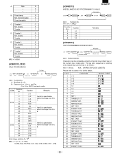
... 0 0 0 1 1 1 0 0 1 1 0 0 0 0 0 0 1 1 * File table No. (Create/Erase) 1,2,3,5 3 4 7,8,9,11 9 10 13 14,15,16,18 16,20 17,22 18 19 20 (or 22) 26,27 28 32,33,34,35,36 40,41 42,43 44 45 6 12 21 (or 23) 31 37 6,12,21 (or 23),31,37 24 25 Type...Daily sales UPC Mix&Match UPC Link Cashier Hourly Daily Net Reg. SERVICE FINAL DEPOSIT DEPOSIT RFND SCALE OPEN TARE INHIBIT ER-A450T KEY POSITION KEY TEXT CONV3 CONV4 FSTEND RA RA2 PO PO2 CASH# BIRTH UPC AMT DEPT# REPEAT INQ NO DEL...38 44 50 56 62 68 37 43 49 55 61 67 R J 04 08 12 16 20 24 28 32 36 42 48 54 60 66 03 07 11 15 19 23 27 31 35 41 47 53 59 65 ...
... 0 0 0 1 1 1 0 0 1 1 0 0 0 0 0 0 1 1 * File table No. (Create/Erase) 1,2,3,5 3 4 7,8,9,11 9 10 13 14,15,16,18 16,20 17,22 18 19 20 (or 22) 26,27 28 32,33,34,35,36 40,41 42,43 44 45 6 12 21 (or 23) 31 37 6,12,21 (or 23),31,37 24 25 Type...Daily sales UPC Mix&Match UPC Link Cashier Hourly Daily Net Reg. SERVICE FINAL DEPOSIT DEPOSIT RFND SCALE OPEN TARE INHIBIT ER-A450T KEY POSITION KEY TEXT CONV3 CONV4 FSTEND RA RA2 PO PO2 CASH# BIRTH UPC AMT DEPT# REPEAT INQ NO DEL...38 44 50 56 62 68 37 43 49 55 61 67 R J 04 08 12 16 20 24 28 32 36 42 48 54 60 66 03 07 11 15 19 23 27 31 35 41 47 53 59 65 ...
Programmer Manual
Page 16
...up 25 UPC X/Z Pick up 26 Mix & Match Table 27 Sales buffer 28 UPC link 29 Transaction Label 30 Daily 31 Term 32 Cashier Preset 33 Flag 34 Text 35 Cashier transaction Label 36 Daily 37 Term 38 Total cashier buffer Label 39 Total 40 Hourly ... 0 *** (14) 1500 *** (14) 0 *** (14) 1500 *** (14) 0 *** (14) 0 *** (14) 0 *** (14) 100 *** 100 *** 0 *** 0 *** (26) 0 *** 89 89 89 89 (29) 89 89 (29) 4 99 4 99 (32) 4 99 (32) 43 43 43 43 (35) 43 43 (35) 43 43 43 43 (38) 48 48 48 48 (40) 36 36 36 36 (42) 80 255...
...up 25 UPC X/Z Pick up 26 Mix & Match Table 27 Sales buffer 28 UPC link 29 Transaction Label 30 Daily 31 Term 32 Cashier Preset 33 Flag 34 Text 35 Cashier transaction Label 36 Daily 37 Term 38 Total cashier buffer Label 39 Total 40 Hourly ... 0 *** (14) 1500 *** (14) 0 *** (14) 1500 *** (14) 0 *** (14) 0 *** (14) 0 *** (14) 100 *** 100 *** 0 *** 0 *** (26) 0 *** 89 89 89 89 (29) 89 89 (29) 4 99 4 99 (32) 4 99 (32) 43 43 43 43 (35) 43 43 (35) 43 43 43 43 (38) 48 48 48 48 (40) 36 36 36 36 (42) 80 255...
Programmer Manual
Page 33
... 82 CH4 84 CH5 Entry range, system: A × 10B MRS = 17 ((-)1-(-)4, TAX) 18 (RA, RA2, PO, PO2, CA1, CA2, CHK, CHK2, CH1 - Function Remarks 1 (-)1 2 3 4 2312 32 (-)2 Item B is specificable within the range from 0 to section 4 for RA/PO and each media JOB# Function No. TAX 64 RA Item B is specificable 65...
... 82 CH4 84 CH5 Entry range, system: A × 10B MRS = 17 ((-)1-(-)4, TAX) 18 (RA, RA2, PO, PO2, CA1, CA2, CHK, CHK2, CH1 - Function Remarks 1 (-)1 2 3 4 2312 32 (-)2 Item B is specificable within the range from 0 to section 4 for RA/PO and each media JOB# Function No. TAX 64 RA Item B is specificable 65...
Programmer Manual
Page 34
F-NO. 30 31 32 33 34 35 36 37 38 39 40 41 42 43 44 45 46 47 48 49 50 51 52 53 54 55 56 57 ...
F-NO. 30 31 32 33 34 35 36 37 38 39 40 41 42 43 44 45 46 47 48 49 50 51 52 53 54 55 56 57 ...
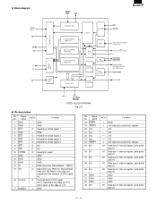
Service Manual
Page 2
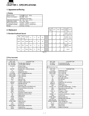
.../Rating 1) Rating Power source Power consumption Operating temperature Operating humidity Physical dimensions, including the drawer Weight 120V 10% AC , 60Hz Standby: 14 W Operating: 37 W (max.) 32 - 104 °F (0°C - 40°C) 10% - 90% (RH) 16.5(W) x 16.8(D) x 11.5(H) in. (420(W) x 427(D) x 292(H)mm) 27.6 lbs ( 13.5 kg...
.../Rating 1) Rating Power source Power consumption Operating temperature Operating humidity Physical dimensions, including the drawer Weight 120V 10% AC , 60Hz Standby: 14 W Operating: 37 W (max.) 32 - 104 °F (0°C - 40°C) 10% - 90% (RH) 16.5(W) x 16.8(D) x 11.5(H) in. (420(W) x 427(D) x 292(H)mm) 27.6 lbs ( 13.5 kg...

Service Manual
Page 10
... VSS 20 A0 21 A1 22 A2 23 A3 24 A4 25 A5 26 A6 27 A7 28 A8 29 A9 30 A10 31 A11 32 A12 33 A13 34 A14 35 A15 36 VSS 37 A16 38 A17 39 A18 40 A19 41 A20 42 A21 43 A22 44 A23...
... VSS 20 A0 21 A1 22 A2 23 A3 24 A4 25 A5 26 A6 27 A7 28 A8 29 A9 30 A10 31 A11 32 A12 33 A13 34 A14 35 A15 36 VSS 37 A16 38 A17 39 A18 40 A19 41 A20 42 A21 43 A22 44 A23...
Service Manual
Page 12
... VSS 21 A0 22 A1 23 A2 24 A3 25 A4 26 A5 27 A6 28 A7 29 A8 30 A9 31 A10 32 A11 33 A12 34 A13 35 A14 36 A15 37 VSS 38 A16 39 A17 40 A18 41 A19 42 A20 43 A21...P53 69 P54 70 P55 71 P56 72 P57 73 P60 /NEJ NU /NER VSS TRG1 /PSTOP /CKDCR2 OPDS FVPON FMRS /SLIPLMP /STOP /ERS 74 P61 75 P62 76 P63 77 P64 /DRS /CSS /CDS /RR 78 P65 /RSS 79 P66 80 P67 81 VSS 82 AVSS ... OUT Nu (GND) OUT Nu (GND) IN Nu (GND) OUT Nu (GND) IN Nu (GND) OUT Nu (GND) OUT Nu (GND) OUT ER signal for RS232 (Equipment Ready) IN DR signal for RS232 (Data set Ready) IN CS signal for RS232 (Clear to Send) IN CD signal for...
... VSS 21 A0 22 A1 23 A2 24 A3 25 A4 26 A5 27 A6 28 A7 29 A8 30 A9 31 A10 32 A11 33 A12 34 A13 35 A14 36 A15 37 VSS 38 A16 39 A17 40 A18 41 A19 42 A20 43 A21...P53 69 P54 70 P55 71 P56 72 P57 73 P60 /NEJ NU /NER VSS TRG1 /PSTOP /CKDCR2 OPDS FVPON FMRS /SLIPLMP /STOP /ERS 74 P61 75 P62 76 P63 77 P64 /DRS /CSS /CDS /RR 78 P65 /RSS 79 P66 80 P67 81 VSS 82 AVSS ... OUT Nu (GND) OUT Nu (GND) IN Nu (GND) OUT Nu (GND) IN Nu (GND) OUT Nu (GND) OUT Nu (GND) OUT ER signal for RS232 (Equipment Ready) IN DR signal for RS232 (Data set Ready) IN CS signal for RS232 (Clear to Send) IN CD signal for...

Service Manual
Page 13
... VCC 20 GND 21 NU 22 VRESC 23 SLTMG 24 SLRST 25 AS 26 RD 27 WR 28 PHAI 29 SDT7 30 SDT6 31 SDT5 32 GND 33 SDT4 34 SDT3 35 SDT2 36 SDT1 37 D0 38 D1 39 D2 40 D3 41 GND 42 D4 43 158 TWAIT D5...
... VCC 20 GND 21 NU 22 VRESC 23 SLTMG 24 SLRST 25 AS 26 RD 27 WR 28 PHAI 29 SDT7 30 SDT6 31 SDT5 32 GND 33 SDT4 34 SDT3 35 SDT2 36 SDT1 37 D0 38 D1 39 D2 40 D3 41 GND 42 D4 43 158 TWAIT D5...

Service Manual
Page 15
... 19 - 20 VCC 21 GND 22 INTMCR 23 VRESC 24 SLTMG 25 SLRST 26 AS 27 RD 28 WR 29 φ 30 SDT7 31 SDT6 32 SDT5 33 GND 34 SDT4 35 SDT3 36 SDT2 37 SDT1 38 D0 39 D1 40 D2 41 D3 42 GND 43 D4 44 D5...
... 19 - 20 VCC 21 GND 22 INTMCR 23 VRESC 24 SLTMG 25 SLRST 26 AS 27 RD 28 WR 29 φ 30 SDT7 31 SDT6 32 SDT5 33 GND 34 SDT4 35 SDT3 36 SDT2 37 SDT1 38 D0 39 D1 40 D2 41 D3 42 GND 43 D4 44 D5...

Service Manual
Page 16
... ST2 20 ST3 21 ST4 22 ST5 23 VDD 24 GND 25 NU 26 KR0 27 KR1 28 KR2 29 KR3 30 KR5 31 KR6 32 2) Pin assignment (CKDC8) Pin No. Nu - Nu - Nu (+5V) -
... ST2 20 ST3 21 ST4 22 ST5 23 VDD 24 GND 25 NU 26 KR0 27 KR1 28 KR2 29 KR3 30 KR5 31 KR6 32 2) Pin assignment (CKDC8) Pin No. Nu - Nu - Nu (+5V) -

Service Manual
Page 17
... (Option) 2. However, the thermalhead composition (the dot number and the block number) is not restricted to the design concept. SYMBOL SIGNAL NAME IN/ OUT FUNCTION 32 KR6 KR6 IN KEY RETURN 6 33 KR7 KR7 IN KEY RETURN 7 34 AVRF GND 35 AVDD VDD 36 /RESET /RES0 IN 37 XT2 38 XT1... 32.768 KHz 39 IC GND 40 X2 41 X1 4.19 MHz 42 VSS1 GND 43 LDRQ LDRQ IN LORD REQUEST 44 ERC ERC IN EVENT ...
... (Option) 2. However, the thermalhead composition (the dot number and the block number) is not restricted to the design concept. SYMBOL SIGNAL NAME IN/ OUT FUNCTION 32 KR6 KR6 IN KEY RETURN 6 33 KR7 KR7 IN KEY RETURN 7 34 AVRF GND 35 AVDD VDD 36 /RESET /RES0 IN 37 XT2 38 XT1... 32.768 KHz 39 IC GND 40 X2 41 X1 4.19 MHz 42 VSS1 GND 43 LDRQ LDRQ IN LORD REQUEST 44 ERC ERC IN EVENT ...

Service Manual
Page 18
... VCC 20 VCC 21 VCC 22 VCC 23 TEST1 24 D0 25 D1 26 D2 27 D3 28 D4 29 GND 30 GND 31 GND 32 D5 33 D6 34 D7 35 A0 36 A1 37 A2 38 NU 39 INTI 40 WI 41 BACK 42 A3 43 158 RESET A4...
... VCC 20 VCC 21 VCC 22 VCC 23 TEST1 24 D0 25 D1 26 D2 27 D3 28 D4 29 GND 30 GND 31 GND 32 D5 33 D6 34 D7 35 A0 36 A1 37 A2 38 NU 39 INTI 40 WI 41 BACK 42 A3 43 158 RESET A4...
Service Manual
Page 19
... TEST2 20 Vcc 21 Vcc 22 Vcc 23 Vcc 24 TEST1 25 D0 26 D1 27 D2 28 D3 29 D4 30 GND 31 GND 32 GND 33 D5 In/Out Function I GND I +5V internal counter timer test pin - +5V - +5V - +5V - +5V I +5V internal counter timer test pin I/O Data bus...
... TEST2 20 Vcc 21 Vcc 22 Vcc 23 Vcc 24 TEST1 25 D0 26 D1 27 D2 28 D3 29 D4 30 GND 31 GND 32 GND 33 D5 In/Out Function I GND I +5V internal counter timer test pin - +5V - +5V - +5V - +5V I +5V internal counter timer test pin I/O Data bus...

Service Manual
Page 21
... VCC 20 GND 21 /CI0 22 /RTS0 23 /CS0 24 /CD1 25 BRK1 26 TRNEMP1 27 RCVRDY1 28 TRNRDY1 29 /CTS1 30 RCVDT1 31 /CI1 32 /RTS1 33 /CS1 34 /CD2 35 TRNEMP2 36 RCVRDY2 37 TRNRDY2 38 CTS2Z 39 RCVDT2 40 120 TRNDTB 119 /CSB 118 GND 117 SYCBKA 116...
... VCC 20 GND 21 /CI0 22 /RTS0 23 /CS0 24 /CD1 25 BRK1 26 TRNEMP1 27 RCVRDY1 28 TRNRDY1 29 /CTS1 30 RCVDT1 31 /CI1 32 /RTS1 33 /CS1 34 /CD2 35 TRNEMP2 36 RCVRDY2 37 TRNRDY2 38 CTS2Z 39 RCVDT2 40 120 TRNDTB 119 /CSB 118 GND 117 SYCBKA 116...

Service Manual
Page 22
Name 1 SL00 2 SL01 3 SL02 4 SL10 5 SL11 6 SL12 7 SL20 8 SL21 9 SL22 10 SL30 11 SL31 12 SL32 ER-A770 VCC GND GND GND GND GND GND GND GND GND GND GND 13 /CD0 /DCD1 14 BRK0 BRK1 15 TRNEMP0 TRENMP1 16 RCVRDY0 RCVRDY1 ... C USART D USART Common input 3) Pin description Pin NO. Name 26 BRK1 27 TRNEMP1 28 RCVRDY1 29 TRNRDY1 30 /CTS1 31 RCVDT1 ER-A770 BRK2 TRENMP2 RCVRDY2 TRNRDY2 /CTS2 RCVDT2 32 /CI1 /CI2 33 /RTS1 /RTS2 34 /CS1 /CS2 35 /CD2 VCC 36 TRNEMP2 TRENMP3 37 RCVRDY2 RCVRDY3 38 TRNRDY2 TRNRDY3 39 CTS2Z...
Name 1 SL00 2 SL01 3 SL02 4 SL10 5 SL11 6 SL12 7 SL20 8 SL21 9 SL22 10 SL30 11 SL31 12 SL32 ER-A770 VCC GND GND GND GND GND GND GND GND GND GND GND 13 /CD0 /DCD1 14 BRK0 BRK1 15 TRNEMP0 TRENMP1 16 RCVRDY0 RCVRDY1 ... C USART D USART Common input 3) Pin description Pin NO. Name 26 BRK1 27 TRNEMP1 28 RCVRDY1 29 TRNRDY1 30 /CTS1 31 RCVDT1 ER-A770 BRK2 TRENMP2 RCVRDY2 TRNRDY2 /CTS2 RCVDT2 32 /CI1 /CI2 33 /RTS1 /RTS2 34 /CS1 /CS2 35 /CD2 VCC 36 TRNEMP2 TRENMP3 37 RCVRDY2 RCVRDY3 38 TRNRDY2 TRNRDY3 39 CTS2Z...
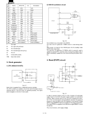
Service Manual
Page 24
...149 150 151 152 153 154 155 156 157 158 159 160 I ID IS ISU IO 3S ON6 Name ER-A770 I/O VCC VCC GND GND /CSD VCC IS TRNDTD NC O /DTRD NC O /RTSD NC O... R116 9.1KG 1SS133 R117 2.7K R118 R119 2.7K 56K 8 3+ B 1 2 - The sub-clock X2 generates 32.768KHz which is turned off program to save the data in the CPU registers in most cases. 2) CKDC8 oscillation circuit 40... X2 CKDC 8 41 X1 37 XT2 38 XT1 HD404728A91FS C106 18P X1 4.19MHz 1 2 3 R164 330K X2 32.768KHz C105 33P Fig. 3-2 Two oscillators are connected to update the internal RTC (real time clock). IC7A 4 ...
...149 150 151 152 153 154 155 156 157 158 159 160 I ID IS ISU IO 3S ON6 Name ER-A770 I/O VCC VCC GND GND /CSD VCC IS TRNDTD NC O /DTRD NC O /RTSD NC O... R116 9.1KG 1SS133 R117 2.7K R118 R119 2.7K 56K 8 3+ B 1 2 - The sub-clock X2 generates 32.768KHz which is turned off program to save the data in the CPU registers in most cases. 2) CKDC8 oscillation circuit 40... X2 CKDC 8 41 X1 37 XT2 38 XT1 HD404728A91FS C106 18P X1 4.19MHz 1 2 3 R164 330K X2 32.768KHz C105 33P Fig. 3-2 Two oscillators are connected to update the internal RTC (real time clock). IC7A 4 ...

Service Manual
Page 27
... the enable register. SSP circuit 1) Block diagram This is the circuit employed for "-----." 3 Lower bits 4 Enable register EN (bit7) = 1 Enable = 0 Inhibit < BAR composition > Fig. 6-4 is 32 entry. FFFF00 7 0 H 1 1 2 2 3 BAR0 3 4 4 5 BAR1 6 7 BAR2 A23~ A0 Control signal ROMCS Fig. 6-2 A19 A18 A17 A16 A15 Fig. 6-3 Each BAR is employed though the mapping system...
... the enable register. SSP circuit 1) Block diagram This is the circuit employed for "-----." 3 Lower bits 4 Enable register EN (bit7) = 1 Enable = 0 Inhibit < BAR composition > Fig. 6-4 is 32 entry. FFFF00 7 0 H 1 1 2 2 3 BAR0 3 4 4 5 BAR1 6 7 BAR2 A23~ A0 Control signal ROMCS Fig. 6-2 A19 A18 A17 A16 A15 Fig. 6-3 Each BAR is employed though the mapping system...
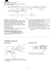
Service Manual
Page 28
...; Drive sequence of each break address register. The break signals (NMI) and the above detection data (CMP0~4) are held until the above detection data are 32 break registers, the binary expression is made in parentheses should not be accessed individually. Information on which break register the SSP break is detected and...
...; Drive sequence of each break address register. The break signals (NMI) and the above detection data (CMP0~4) are held until the above detection data are 32 break registers, the binary expression is made in parentheses should not be accessed individually. Information on which break register the SSP break is detected and...
Service Manual
Page 32
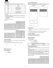
...26 R J 3F 3E 3D 34 33 3C 28 2D 23 2E 2F 25 A4 2B 21 2A 20 29 1F 32 1E 4C 4B 24 1C 1B 0E 17 18 16 48 15 47 14 46 0F 05 10 11 12 04 ... 57 48 38 R J 63 62 61 52 51 60 40 45 35 46 47 37 74 43 33 42 32 41 31 49 30 76 75 36 28 27 14 23 24 22 72 21 71 20 70 15 05 16 ...12 02 11 01 10 00 26 25 06 07 08 R J 63 62 61 52 51 74 43 33 42 32 41 31 14 23 24 22 72 21 71 04 13 03 12 02 11 01 65 68 67 58 77 ... [4] Keyboard test 1) Key operation XXXX 104 CA/AT XXXX: Sumcheck data Standard keyboard layout sum check data ER-A450T 2254 2) Functional description The keyboard test is terminated automatically.
...26 R J 3F 3E 3D 34 33 3C 28 2D 23 2E 2F 25 A4 2B 21 2A 20 29 1F 32 1E 4C 4B 24 1C 1B 0E 17 18 16 48 15 47 14 46 0F 05 10 11 12 04 ... 57 48 38 R J 63 62 61 52 51 60 40 45 35 46 47 37 74 43 33 42 32 41 31 49 30 76 75 36 28 27 14 23 24 22 72 21 71 20 70 15 05 16 ...12 02 11 01 10 00 26 25 06 07 08 R J 63 62 61 52 51 74 43 33 42 32 41 31 14 23 24 22 72 21 71 04 13 03 12 02 11 01 65 68 67 58 77 ... [4] Keyboard test 1) Key operation XXXX 104 CA/AT XXXX: Sumcheck data Standard keyboard layout sum check data ER-A450T 2254 2) Functional description The keyboard test is terminated automatically.


