Service Manual
Page 1
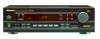
BLOCK DIAGRAM AND SCHEMATIC DIAGRAM ..... 6 4. GENERAL INFORMATION 26 7.1 PARTS 26 7.1.1 IC 26 7.1.2 DISPLAY 33 8. PIONEER ELECTRONIC (EUROPE) N.V. Haven 1087, Keetberglaan 1, 9120 Melsele, Belgium PIONEER ELECTRONICS ASIACENTRE PTE. CHANNEL RECEIVER VSX-108 ORDER NO. P.O. LTD. 253 Alexandra Road, #04-01, Singapore 159936 c PIONEER CORPORATION 1999 T - AUDIO MULTI - PCB CONNECTION DIAGRAM 17 5. PANEL FACILITIES AND SPECIFICATIONS ....... 35 PIONEER CORPORATION 4-1, Meguro 1-chome...
BLOCK DIAGRAM AND SCHEMATIC DIAGRAM ..... 6 4. GENERAL INFORMATION 26 7.1 PARTS 26 7.1.1 IC 26 7.1.2 DISPLAY 33 8. PIONEER ELECTRONIC (EUROPE) N.V. Haven 1087, Keetberglaan 1, 9120 Melsele, Belgium PIONEER ELECTRONICS ASIACENTRE PTE. CHANNEL RECEIVER VSX-108 ORDER NO. P.O. LTD. 253 Alexandra Road, #04-01, Singapore 159936 c PIONEER CORPORATION 1999 T - AUDIO MULTI - PCB CONNECTION DIAGRAM 17 5. PANEL FACILITIES AND SPECIFICATIONS ....... 35 PIONEER CORPORATION 4-1, Meguro 1-chome...

Service Manual
Page 2
...Health & Safety Code Section 25249.6 - For the latest information, always consult the current PIONEER Service Manual. SAFETY INFORMATION This service manual is continuously under test Reading should be above 0....Electrical components having such features are known to the state of this Service Manual. VSX-108 1. SAFETY PRECAUTIONS The following check should Leakage current not be performed for the ... the earth ground and all exposed metal surfaces Also test with a on the schematics and on the parts list in the appliance have these special safety characteristics are ...
...Health & Safety Code Section 25249.6 - For the latest information, always consult the current PIONEER Service Manual. SAFETY INFORMATION This service manual is continuously under test Reading should be above 0....Electrical components having such features are known to the state of this Service Manual. VSX-108 1. SAFETY PRECAUTIONS The following check should Leakage current not be performed for the ... the earth ground and all exposed metal surfaces Also test with a on the schematics and on the parts list in the appliance have these special safety characteristics are ...
Service Manual
Page 6
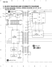
1 2 3 4 VSX-108 3. CN702 1 2 3 4 5 6 7 DATA CLK E1 DATA CLK E2 DGND CN6 1 2 3 4 5 6...8V -25V +5V GND SR GND CN7 1 2 3 4 5 6 7 B MAIN PCB B 1/2, B 2/2 V1 FL TUBE 04991693-001 1 2 CONTROL OUT IC703 06104421-000 D IR Receiver G DISPLAY PCB 6 1 2 3 4 GND AM/FM IF 12 10 9 8 7 6 5 4 3 2 1 L B CN708 CN701 TV R L VCR IN R 75 FM IN... VCR OUT R 61 62 24 21 DATA 9 DATA 50 IC701 00272358-040 (LC72358N) Control µ-Com. BLOCK DIAGRAM AND SCHEMATIC DIAGRAM 3.1 BLOCK DIAGRAM, OVERALL WIRING DIAGRAM, AC O/P, AC I/P A and PW SW PCBS FM ANTENNA AM ANTENNA A TUNER ...
1 2 3 4 VSX-108 3. CN702 1 2 3 4 5 6 7 DATA CLK E1 DATA CLK E2 DGND CN6 1 2 3 4 5 6...8V -25V +5V GND SR GND CN7 1 2 3 4 5 6 7 B MAIN PCB B 1/2, B 2/2 V1 FL TUBE 04991693-001 1 2 CONTROL OUT IC703 06104421-000 D IR Receiver G DISPLAY PCB 6 1 2 3 4 GND AM/FM IF 12 10 9 8 7 6 5 4 3 2 1 L B CN708 CN701 TV R L VCR IN R 75 FM IN... VCR OUT R 61 62 24 21 DATA 9 DATA 50 IC701 00272358-040 (LC72358N) Control µ-Com. BLOCK DIAGRAM AND SCHEMATIC DIAGRAM 3.1 BLOCK DIAGRAM, OVERALL WIRING DIAGRAM, AC O/P, AC I/P A and PW SW PCBS FM ANTENNA AM ANTENNA A TUNER ...
Service Manual
Page 17
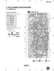
... for several destinations. 1 2 3 4 VSX-108 4. Part numbers in PCB diagrams match those in the schematic diagrams. 2. Symbol In PCB Diagrams Symbol In Schematic Diagrams B C EB C E Part Name BCE Transistor BCE B C EB C E Transistor with the schematic diagram. 4. PCB CONNECTION DIAGRAM 4.1 TUNER ... SD G S Field effect transistor A TUNER PCB Resistor array 3-terminal regulator Q102 B 3. View point of PCB and schematic diagrams is shown below. A comparison between the main parts of PCB diagrams. IC101 Connector Capacitor Q101 SIDE A Q103 P.C.Board...
... for several destinations. 1 2 3 4 VSX-108 4. Part numbers in PCB diagrams match those in the schematic diagrams. 2. Symbol In PCB Diagrams Symbol In Schematic Diagrams B C EB C E Part Name BCE Transistor BCE B C EB C E Transistor with the schematic diagram. 4. PCB CONNECTION DIAGRAM 4.1 TUNER ... SD G S Field effect transistor A TUNER PCB Resistor array 3-terminal regulator Q102 B 3. View point of PCB and schematic diagrams is shown below. A comparison between the main parts of PCB diagrams. IC101 Connector Capacitor Q101 SIDE A Q103 P.C.Board...
Service Manual
Page 26
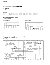
... AMP. GENERAL INFORMATION 7.1 PARTS 7.1.1 IC • The information shown in the list is basic information and may not correspond exactly to that shown in the schematic diagrams. •List of IC LA1186N, STK407-070, 00201838-040 (LA1838), 00206458-040 (LA6458S), 00201041-040 (LV1041M), 00262419-010 (M62419FP), 00272358-040 (LC72358N), 00202879-040.... STEREO SW MUTE SD COMP AM IF DET AM S-METER FF 304kHz FF FF 38k 19k∠π/θ FF 19k∠θ PILOT DET. VSX-108 7. AM OSC REG.
... AMP. GENERAL INFORMATION 7.1 PARTS 7.1.1 IC • The information shown in the list is basic information and may not correspond exactly to that shown in the schematic diagrams. •List of IC LA1186N, STK407-070, 00201838-040 (LA1838), 00206458-040 (LA6458S), 00201041-040 (LV1041M), 00262419-010 (M62419FP), 00272358-040 (LC72358N), 00202879-040.... STEREO SW MUTE SD COMP AM IF DET AM S-METER FF 304kHz FF FF 38k 19k∠π/θ FF 19k∠θ PILOT DET. VSX-108 7. AM OSC REG.
