AXM751 Install Guide
Page 1
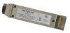
Installing a AXM751 Module Insert the module firmly into an available module slot. Specifications Standard Dimensions (HxWxD) Weight Operating Temperature IEEE 802.3ae 10GBase...mode LC to LC duplex cable. Removing a AXM751 Module Release the module latch by pulling down the handle bar across the module, and pull the module out of the module slot. )NSTALLATION'UIDE XFP GBIC Module AXM751 The 10 Gigabit small form-factor pluggable (XFP) module provides a full-duplex 10G bps Ethernet link on NETGEAR managed switches. The module can simply plug it into the slot that supports the XFP...
Installing a AXM751 Module Insert the module firmly into an available module slot. Specifications Standard Dimensions (HxWxD) Weight Operating Temperature IEEE 802.3ae 10GBase...mode LC to LC duplex cable. Removing a AXM751 Module Release the module latch by pulling down the handle bar across the module, and pull the module out of the module slot. )NSTALLATION'UIDE XFP GBIC Module AXM751 The 10 Gigabit small form-factor pluggable (XFP) module provides a full-duplex 10G bps Ethernet link on NETGEAR managed switches. The module can simply plug it into the slot that supports the XFP...
AXM751 Install Guide
Page 2
... of the port when no fiber cable is a registered trademark of NETGEAR, Inc. Federal Office for Telecommunications Approvals has being granted the right to test the series for a Class B digital device, pursuant to change the product described in the operating instructions. June 6, 2006 This symbol was placed in a commercial installation. If disposed of within...
... of the port when no fiber cable is a registered trademark of NETGEAR, Inc. Federal Office for Telecommunications Approvals has being granted the right to test the series for a Class B digital device, pursuant to change the product described in the operating instructions. June 6, 2006 This symbol was placed in a commercial installation. If disposed of within...
AXM751 Product Datasheet
Page 2
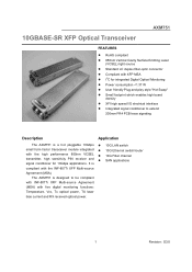
AXM751 10GBASE-SR XFP Optical Transceiver FEATURES RoHS compliant 850nm Vertical Cavity Surface Emitting Laser (VCSEL) light source Standard LC duplex fiber-optic connector Compliant with XFP MSA I2C for integrated Digital Optical Monitoring Power consumption
AXM751 10GBASE-SR XFP Optical Transceiver FEATURES RoHS compliant 850nm Vertical Cavity Surface Emitting Laser (VCSEL) light source Standard LC duplex fiber-optic connector Compliant with XFP MSA I2C for integrated Digital Optical Monitoring Power consumption
AXM751 Product Datasheet
Page 3
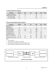
...The data rate of input data is 10.3125Gb/s 3. 1. Non-condensing 2. RD- 500 650 Notes: 1. Input voltage swing (differential) measured peak-to -peak AXM751 Max Units Notes 85 °C 90 % 6.0 V 3.6 V Max 70 85 3.465 5.25 350 30 1.37 1000 800 Units Notes °C % [1]... V V mA mA W mVp-p [2,3] mVp-p [4] ASIC / SerDes XFP XFP ASIC / SerDes 10Gbps XFI electrical signal 10Gbps optical signal Application Block Diagram 10Gbps XFI electrical signal 2 Revision: S3.0 Absolute Maximum Ratings Parameter Symbol ...
...The data rate of input data is 10.3125Gb/s 3. 1. Non-condensing 2. RD- 500 650 Notes: 1. Input voltage swing (differential) measured peak-to -peak AXM751 Max Units Notes 85 °C 90 % 6.0 V 3.6 V Max 70 85 3.465 5.25 350 30 1.37 1000 800 Units Notes °C % [1]... V V mA mA W mVp-p [2,3] mVp-p [4] ASIC / SerDes XFP XFP ASIC / SerDes 10Gbps XFI electrical signal 10Gbps optical signal Application Block Diagram 10Gbps XFI electrical signal 2 Revision: S3.0 Absolute Maximum Ratings Parameter Symbol ...

AXM751 Product Datasheet
Page 4
...25, 0.28, 0.40} Gb/s ppm dBm nm nm dBm dB dBm dB/Hz dB Transmitter eye mask definition Notes Minimum optical modulation amplitude (dBm) relation table Center RMS Specrtal width (nm) Wavelength Up to 0.05 to 0.1 to 0.15 to 0.2 to 0.... -3.8 -3.6 -3.3 -3.0 850 to 852 -4.3 -4.2 -4.2 -4.1 -4.0 -3.8 -3.6 -3.4 -3.0 852 to 854 -4.3 -4.2 -4.2 -4.1 -4.0 -3.9 -3.7 -3.4 -3.1 854 to 856 -4.3 -4.3 -4.2 -4.1 -4.0 -3.9 -3.7 -3.4 -3.1 856 to 858 -4.3 -4.3 -4.2 -4.1 -4.0 -3.9 -3.7 -3.5 -3.1 858 to 860 -4.3 -4.3 -4.2 -4.2 -4.1 -3.9 -3.7 -3.5 -3.2 Triple tradeoff curve 3 Revision: S3.0 AXM751 3.
...25, 0.28, 0.40} Gb/s ppm dBm nm nm dBm dB dBm dB/Hz dB Transmitter eye mask definition Notes Minimum optical modulation amplitude (dBm) relation table Center RMS Specrtal width (nm) Wavelength Up to 0.05 to 0.1 to 0.15 to 0.2 to 0.... -3.8 -3.6 -3.3 -3.0 850 to 852 -4.3 -4.2 -4.2 -4.1 -4.0 -3.8 -3.6 -3.4 -3.0 852 to 854 -4.3 -4.2 -4.2 -4.1 -4.0 -3.9 -3.7 -3.4 -3.1 854 to 856 -4.3 -4.3 -4.2 -4.1 -4.0 -3.9 -3.7 -3.4 -3.1 856 to 858 -4.3 -4.3 -4.2 -4.1 -4.0 -3.9 -3.7 -3.5 -3.1 858 to 860 -4.3 -4.3 -4.2 -4.2 -4.1 -3.9 -3.7 -3.5 -3.2 Triple tradeoff curve 3 Revision: S3.0 AXM751 3.

AXM751 Product Datasheet
Page 5
XFI Module Receiver Output Jitter Specifications at 10−12 BER 2. Optical Receive Characteristics (TA=0 ºC to 70 ºC) Parameter Symbol Min Typ Max Units Notes Signaling speed (nominal) Ts Signaling ... of the optical signal with 4.75dB extinction ratio at C' Parameter - C' Symbol Min Typ Max 4 Units Notes Revision: S3.0 When the terminal is Low-level (fixed) 3. AXM751 4. When LOS asserted, the data output is viewed from nominal Center Wavelength λ 840 Overload Receiver sensitivity in OMA PO RSO LOS De-assert LOS...
XFI Module Receiver Output Jitter Specifications at 10−12 BER 2. Optical Receive Characteristics (TA=0 ºC to 70 ºC) Parameter Symbol Min Typ Max Units Notes Signaling speed (nominal) Ts Signaling ... of the optical signal with 4.75dB extinction ratio at C' Parameter - C' Symbol Min Typ Max 4 Units Notes Revision: S3.0 When the terminal is Low-level (fixed) 3. AXM751 4. When LOS asserted, the data output is viewed from nominal Center Wavelength λ 840 Overload Receiver sensitivity in OMA PO RSO LOS De-assert LOS...

AXM751 Product Datasheet
Page 6
XFI Module Receiver Differential Output Compliance Mask XFI Termination and AC Coupling 5 Revision: S3.0 Includes jitter transferred from the optical receiver during any valid operational input condition. AXM751 Deterministic Jitter Total Jitter Eye Mask DJ TJ X1 X2 Y1 170 Y2 0.18 UI (p-p) [1] 0.34 UI (p-p) [1] 0.17 UI 0.42 UI mV 425 mV Notes: 1.
XFI Module Receiver Differential Output Compliance Mask XFI Termination and AC Coupling 5 Revision: S3.0 Includes jitter transferred from the optical receiver during any valid operational input condition. AXM751 Deterministic Jitter Total Jitter Eye Mask DJ TJ X1 X2 Y1 170 Y2 0.18 UI (p-p) [1] 0.34 UI (p-p) [1] 0.17 UI 0.42 UI mV 425 mV Notes: 1.
AXM751 Product Datasheet
Page 7
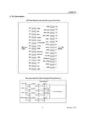
6. Pin Description XFP Host Board Connector Pad Layout (Top View) AXM751 Recommended Host Board Supply Filtering Network 6 Revision: S3.0
6. Pin Description XFP Host Board Connector Pad Layout (Top View) AXM751 Recommended Host Board Supply Filtering Network 6 Revision: S3.0

AXM751 Product Datasheet
Page 8
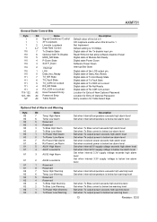
AXM751 Module Electrical Pin Function Definition Pin Logic Symbol Name/Description Note 1 GND Module Ground [1] 2 VEE5 Optional -5.2V Power Supply --Not Required Module De-select; Grounded in the low power mode. 22 VCC2 +1.8V Power Supply --Not Required 23 GND Module Ground [1] 24 PECL-I Mod_DeSel 2-wire serial interface Interrupt Bar; Indicating Module Operational Fault [2] 14 LVTTL-O RX_LOS Receiver...
AXM751 Module Electrical Pin Function Definition Pin Logic Symbol Name/Description Note 1 GND Module Ground [1] 2 VEE5 Optional -5.2V Power Supply --Not Required Module De-select; Grounded in the low power mode. 22 VCC2 +1.8V Power Supply --Not Required 23 GND Module Ground [1] 24 PECL-I Mod_DeSel 2-wire serial interface Interrupt Bar; Indicating Module Operational Fault [2] 14 LVTTL-O RX_LOS Receiver...

AXM751 Product Datasheet
Page 9
...is then asserted "High" when the XFP module is an input pin. When the... XFP modules are met. 3 INTERRUPT Interrupt is "High", the module shall not respond to Host_Vcc on a single ...XFP modules on the host board. 8 Revision: S3.0 The TX_DIS pin must be pulled up to the 2-wire serial interface the XFP module... ‧ Receiver Signal Conditioner Loss of different modules may overlap as long as the above timing ...XFP module. 5 MOD_ABS Mod_ABS is an input pin. The RX_LOS pin is asserted High, the XFP module transmitter output must be turned off. When held Low by the host, the module...
...is then asserted "High" when the XFP module is an input pin. When the... XFP modules are met. 3 INTERRUPT Interrupt is "High", the module shall not respond to Host_Vcc on a single ...XFP modules on the host board. 8 Revision: S3.0 The TX_DIS pin must be pulled up to the 2-wire serial interface the XFP module... ‧ Receiver Signal Conditioner Loss of different modules may overlap as long as the above timing ...XFP module. 5 MOD_ABS Mod_ABS is an input pin. The RX_LOS pin is asserted High, the XFP module transmitter output must be turned off. When held Low by the host, the module...
AXM751 Product Datasheet
Page 10
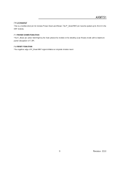
AXM751 7 P_DOWN/RST This is a multifunction pin for module Power Down and Reset. The P_Down/RST pin must be pulled up to VCC3 in the XFP module. 7.1 POWER DOWN FUNCTION The P_Down pin, when held High by the host, places the module in the standby (Low Power) mode with a maximum power dissipation of 1.5W. 7.2 RESET FUNCTION The negative edge of P_Down/RST signal initiates a complete module reset. 9 Revision: S3.0
AXM751 7 P_DOWN/RST This is a multifunction pin for module Power Down and Reset. The P_Down/RST pin must be pulled up to VCC3 in the XFP module. 7.1 POWER DOWN FUNCTION The P_Down pin, when held High by the host, places the module in the standby (Low Power) mode with a maximum power dissipation of 1.5W. 7.2 RESET FUNCTION The negative edge of P_Down/RST signal initiates a complete module reset. 9 Revision: S3.0
AXM751 Product Datasheet
Page 11
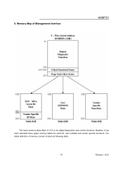
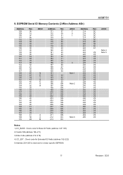
The detail definition of Management Interface AXM751 The lower memory table (Byte 0~127) is listed as following table. 10 Revision: S3.0 Memory Map of memory content is for serial ID, user writable and vendor specific functions. Besides, it has been allocated three upper memory tables for digital diagnostics and control functions. 8.
The detail definition of Management Interface AXM751 The lower memory table (Byte 0~127) is listed as following table. 10 Revision: S3.0 Memory Map of memory content is for serial ID, user writable and vendor specific functions. Besides, it has been allocated three upper memory tables for digital diagnostics and control functions. 8.
AXM751 Product Datasheet
Page 12
... 231 232 233 234 235 236 237 238 239 240 241 242 243 244 245 246 247 248 249 250 251 252 253 254 255 AXM751 Hex ASCII DC DC DC DC DC DC 08 60 67 Note 4 VS Note 5 VS VS VS VS VS VS VS VS VS VS VS... VS VS VS VS VS VS VS VS VS VS VS Notes: 1) CC_BASE : Check code for Base ID Fields (address 120~190) 2) Vendor SN (address 196-211) 3) Date Code (address 212-219) 4) CC_EXT : Check code for Extended ID Fields (address 192~222) 5) Address 224~255 is reserved for vendor specific EEPROM 11 Revision: S3.0
... 231 232 233 234 235 236 237 238 239 240 241 242 243 244 245 246 247 248 249 250 251 252 253 254 255 AXM751 Hex ASCII DC DC DC DC DC DC 08 60 67 Note 4 VS Note 5 VS VS VS VS VS VS VS VS VS VS VS... VS VS VS VS VS VS VS VS VS VS VS Notes: 1) CC_BASE : Check code for Base ID Fields (address 120~190) 2) Vendor SN (address 196-211) 3) Date Code (address 212-219) 4) CC_EXT : Check code for Extended ID Fields (address 192~222) 5) Address 224~255 is reserved for vendor specific EEPROM 11 Revision: S3.0
AXM751 Product Datasheet
Page 13
... (3.3V) 1) P: Operating optical power of transmitter at room temperature Value (Dec.) 85 -10 80 -5 Iop+10 mA Iop-5 mA Iop+7 mA Iop-3 mA P+3 P -3 P +2 P -2 0 -13.1 -1 -11.1 5.5 4.5 5.3 4.7 3.6 3.0 3.5 3.1 AXM751 Unit ℃ mA dBm dBm Volt Volt 12 Revision: S3.0
... (3.3V) 1) P: Operating optical power of transmitter at room temperature Value (Dec.) 85 -10 80 -5 Iop+10 mA Iop-5 mA Iop+7 mA Iop-3 mA P+3 P -3 P +2 P -2 0 -13.1 -1 -11.1 5.5 4.5 5.3 4.7 3.6 3.0 3.5 3.1 AXM751 Unit ℃ mA dBm dBm Volt Volt 12 Revision: S3.0
AXM751 Product Datasheet
Page 14
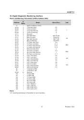
AXM751 General State/ Control Bits Byte 1 1 1 1 110 110 110 110 110 110 110 110 111 111 111 ... Ready Digital state of Rx CDR not Locked Location for Entry of New Optional Password Location for Entry of Optional Password Entry Location for Table Select Byte Optional Set of Alarm and Warning Byte 80 80 80 80 80 80 80 80 81 ... software disable of laser Digital state of Module Not Ready Digital state Power Down Software Power Down Interrupt Bar State Digital state of this bit is 0 XFI loopback enable when this bit set to 1 Not Implement Default setting is below low warning level 13 Revision:...
AXM751 General State/ Control Bits Byte 1 1 1 1 110 110 110 110 110 110 110 110 111 111 111 ... Ready Digital state of Rx CDR not Locked Location for Entry of New Optional Password Location for Entry of Optional Password Entry Location for Table Select Byte Optional Set of Alarm and Warning Byte 80 80 80 80 80 80 80 80 81 ... software disable of laser Digital state of Module Not Ready Digital state Power Down Software Power Down Interrupt Bar State Digital state of this bit is 0 XFI loopback enable when this bit set to 1 Not Implement Default setting is below low warning level 13 Revision:...
AXM751 Product Datasheet
Page 15
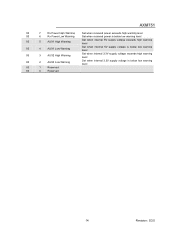
AXM751 83 7 Rx Power High Warning Set when received power exceeds high warning level 83 6 Rx Power Low Warning Set when received power is below low warning level 83 5 AUX1 High Warning Set when internal 5V supply voltage exceeds high warning level 83 4 AUX1 Low Warning Set when internal 5V supply voltage is below low warning level 83 3 AUX2 High Warning Set when internal 3.3V supply voltage exceeds high warning level 83 2 AUX2 Low Warning Set when internal 3.3V supply voltage is below low warning level 83 1 Reserved 83 0 Reserved 14 Revision: S3.0
AXM751 83 7 Rx Power High Warning Set when received power exceeds high warning level 83 6 Rx Power Low Warning Set when received power is below low warning level 83 5 AUX1 High Warning Set when internal 5V supply voltage exceeds high warning level 83 4 AUX1 Low Warning Set when internal 5V supply voltage is below low warning level 83 3 AUX2 High Warning Set when internal 3.3V supply voltage exceeds high warning level 83 2 AUX2 Low Warning Set when internal 3.3V supply voltage is below low warning level 83 1 Reserved 83 0 Reserved 14 Revision: S3.0
AXM751 Product Datasheet
Page 16
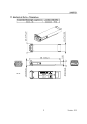
11. Mechanical Outline Dimensions Transmitter Wavelength / Application Latch Color Identifier 850nm / SR Beige AXM751 272-10563-01 AXM751 Complies with 21 CFR 1040.10 and 1040.11 Multi Mode/850nm 10Gbps 10GBase-SR R Made in Taiwan 15 Revision: S3.0
11. Mechanical Outline Dimensions Transmitter Wavelength / Application Latch Color Identifier 850nm / SR Beige AXM751 272-10563-01 AXM751 Complies with 21 CFR 1040.10 and 1040.11 Multi Mode/850nm 10Gbps 10GBase-SR R Made in Taiwan 15 Revision: S3.0
AXM751 Product Datasheet
Page 17
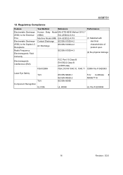
...STD-883E Method 3015.7 (HBM) EIA-JESD22-A114 Machine Model (MM) EIA-JESD22-A115 (1) Satisfied with Contact Discharge IEC/EN 61000-4-2 electrical Air Discharge IEC/EN 61000-4-2 characteristics of product spec. IEC/EN 61000-4-3 (2) No physical damage FDA/CDRH FCC Part 15 Class B EN 55022 Class B (CISPR 22A)... FDA 21CFR 1040.10, 1040.11 CDRH File # 0420993 Laser Eye Safety TUV TUV Component Recognition UL/CSA IEC/EN 60825-1 IEC/EN 60825-2 IEC/EN 60950 UL 60950 TUV Certificate # R50067719 UL File # E239394 16 Revision: S3.0 AXM751...
...STD-883E Method 3015.7 (HBM) EIA-JESD22-A114 Machine Model (MM) EIA-JESD22-A115 (1) Satisfied with Contact Discharge IEC/EN 61000-4-2 electrical Air Discharge IEC/EN 61000-4-2 characteristics of product spec. IEC/EN 61000-4-3 (2) No physical damage FDA/CDRH FCC Part 15 Class B EN 55022 Class B (CISPR 22A)... FDA 21CFR 1040.10, 1040.11 CDRH File # 0420993 Laser Eye Safety TUV TUV Component Recognition UL/CSA IEC/EN 60825-1 IEC/EN 60825-2 IEC/EN 60950 UL 60950 TUV Certificate # R50067719 UL File # E239394 16 Revision: S3.0 AXM751...
AXM751 Product Datasheet
Page 18
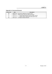
S0 S1 S2 S3 Date 2006-04-25 2006-06-16 2006-08-25 2007-09-27 Description Preliminary datasheet for RoHS version Update product label and safety description 1. Update module characteristics and Latch Color 1.Change the label dimension AXM751 17 Revision: S3.0 Appendix A. Update Digital Diagnostic Memory Map contents 2. Document Revision Version No.
S0 S1 S2 S3 Date 2006-04-25 2006-06-16 2006-08-25 2007-09-27 Description Preliminary datasheet for RoHS version Update product label and safety description 1. Update module characteristics and Latch Color 1.Change the label dimension AXM751 17 Revision: S3.0 Appendix A. Update Digital Diagnostic Memory Map contents 2. Document Revision Version No.

AXM751 Product Datasheet
Page 19
D-AXM751-0 All rights reserved. Information is subject to change without notice. © 2008 NETGEAR, Inc. in the United States and/or other countries. Other brand names mentioned herein are trademarks of their respective holder(s). NETGEAR, the NETGEAR Logo, NETGEAR Digital Entertainer Logo, Connect with Innovation, FrontView, IntelliFi, PowerShift, ProSafe, RAIDar, RAIDiator, X-RAID, RangeMax, ReadyNAS and Smart Wizard are for identification purposes only and may be trademarks of NETGEAR, Inc.
D-AXM751-0 All rights reserved. Information is subject to change without notice. © 2008 NETGEAR, Inc. in the United States and/or other countries. Other brand names mentioned herein are trademarks of their respective holder(s). NETGEAR, the NETGEAR Logo, NETGEAR Digital Entertainer Logo, Connect with Innovation, FrontView, IntelliFi, PowerShift, ProSafe, RAIDar, RAIDiator, X-RAID, RangeMax, ReadyNAS and Smart Wizard are for identification purposes only and may be trademarks of NETGEAR, Inc.