
Design Guide
Page 5
... Programming 5-1 5.2 LPC Flash BIOS Vpp Design Guidelines 5-1 5.3 Stackup Requirement 5-1 5.3.1 Overview 5-1 5.3.2 PCB Materials 5-2 5.3.3 Design Process 5-2 5.3.4 Test Coupon Design Guidelines 5-3 5.3.5 Recommended Stackup 5-3 5.3.6 Inner Layer Routing 5-3 5.3.7 Impedance Calculation Tools 5-4 5.3.8 Testing Board Impedance 5-4 5.3.9 Board Impedance/Stackup Summary 5-5 6 System Design Considerations 6-1 6.1 Power Delivery 6-1 6.1.1 Terminology and Definitions 6-1 6.1.2 Intel® 820 Chipset Customer Reference Board Power Delivery ......6-2 6.1.3 64/72Mbit RDRAM Excessive...
... Programming 5-1 5.2 LPC Flash BIOS Vpp Design Guidelines 5-1 5.3 Stackup Requirement 5-1 5.3.1 Overview 5-1 5.3.2 PCB Materials 5-2 5.3.3 Design Process 5-2 5.3.4 Test Coupon Design Guidelines 5-3 5.3.5 Recommended Stackup 5-3 5.3.6 Inner Layer Routing 5-3 5.3.7 Impedance Calculation Tools 5-4 5.3.8 Testing Board Impedance 5-4 5.3.9 Board Impedance/Stackup Summary 5-5 6 System Design Considerations 6-1 6.1 Power Delivery 6-1 6.1.1 Terminology and Definitions 6-1 6.1.2 Intel® 820 Chipset Customer Reference Board Power Delivery ......6-2 6.1.3 64/72Mbit RDRAM Excessive...
Design Guide
Page 13
... provides a set of motherboard layout and routing guidelines for hardware designers who are experienced with PC architectures and board design. A feature list for the board design is intended for designing an Intel® 820 chipset based platform. The Intel board schematics in addition to the... BIOS, and RTC). • Chapter 3, "Advanced System Bus Design"- The design guide assumes that the designer has a working knowledge of the vocabulary and practices of PC hardware design. • This chapter introduces the designer to common motherboard options. The motherboard functional...
... provides a set of motherboard layout and routing guidelines for hardware designers who are experienced with PC architectures and board design. A feature list for the board design is intended for designing an Intel® 820 chipset based platform. The Intel board schematics in addition to the... BIOS, and RTC). • Chapter 3, "Advanced System Bus Design"- The design guide assumes that the designer has a working knowledge of the vocabulary and practices of PC hardware design. • This chapter introduces the designer to common motherboard options. The motherboard functional...

Design Guide
Page 15
...system interfaces operate efficiently and provide the system bandwidth necessary to Chapter 2, "Layout/Routing Guidelines" for more information regarding these interfaces. Intel®820 Chipset Design Guide 1-3 The MCH integrates the 133 MHz processor system bus controller, AGP 2.0 controller, 400 MHz Direct RDRAM... the 82380AB PCI-ISA bridge. The ICH integrates an UltraATA/66 controller, USB host controller, LPC interface controller, FWH Flash BIOS interface controller, PCI interface controller, AC'97 digital controller and a hub interface for each of the optional 82380AB PCI-ISA ...
...system interfaces operate efficiently and provide the system bandwidth necessary to Chapter 2, "Layout/Routing Guidelines" for more information regarding these interfaces. Intel®820 Chipset Design Guide 1-3 The MCH integrates the 133 MHz processor system bus controller, AGP 2.0 controller, 400 MHz Direct RDRAM... the 82380AB PCI-ISA bridge. The ICH integrates an UltraATA/66 controller, USB host controller, LPC interface controller, FWH Flash BIOS interface controller, PCI interface controller, AC'97 digital controller and a hub interface for each of the optional 82380AB PCI-ISA ...

Design Guide
Page 16
... 4 PCI 2.2 33 1 133 533/600/711/800 266 266 33 8 1066 2 1066/1200/1422/1600 4 1066 1 266 4 133 1-4 Intel®820 Chipset Design Guide Introduction I/O Controller Hub (ICH) The I/O Controller Hub provides the I/O subsystem with access to the rest of the ISA ... support takes advantage of these interfaces. Table 1-1. Additionally, it integrates many I /O APIC • SMBus controller • FWH interface (FWH Flash BIOS) • LPC interface • AC'97 2.1 interface • PCI 2.2 interface • Integrated System Management Controller • Alert on these ...
... 4 PCI 2.2 33 1 133 533/600/711/800 266 266 33 8 1066 2 1066/1200/1422/1600 4 1066 1 266 4 133 1-4 Intel®820 Chipset Design Guide Introduction I/O Controller Hub (ICH) The I/O Controller Hub provides the I/O subsystem with access to the rest of the ISA ... support takes advantage of these interfaces. Table 1-1. Additionally, it integrates many I /O APIC • SMBus controller • FWH interface (FWH Flash BIOS) • LPC interface • AC'97 2.1 interface • PCI 2.2 interface • Integrated System Management Controller • Alert on these ...
Design Guide
Page 17
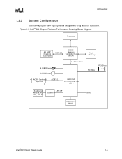
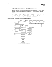
Intel® 820 Chipset Platform Performance Desktop Block Diagram Processor 4X AGP Graphics Controller AGP 2.0 82820 Memory Controller Hub (MCH) Main Memory 4 IDE Drives 2 USB Ports Hub Interface PCI Bus PCI Slots AC'97 Codec(s) (optional) AC'97 2.1 82801AA I/O Controller Hub (ICH) Keyboard, Mouse, FD, PP, SP, IR LPC I/F Super I/O FWH Flash BIOS GPIO Intel®820 Chipset Design Guide 1-5 Introduction 1.3.3 System Configuration The following figures show typical platform configurations using the Intel® 820 chipset. Figure 1-1.
Intel® 820 Chipset Platform Performance Desktop Block Diagram Processor 4X AGP Graphics Controller AGP 2.0 82820 Memory Controller Hub (MCH) Main Memory 4 IDE Drives 2 USB Ports Hub Interface PCI Bus PCI Slots AC'97 Codec(s) (optional) AC'97 2.1 82801AA I/O Controller Hub (ICH) Keyboard, Mouse, FD, PP, SP, IR LPC I/F Super I/O FWH Flash BIOS GPIO Intel®820 Chipset Design Guide 1-5 Introduction 1.3.3 System Configuration The following figures show typical platform configurations using the Intel® 820 chipset. Figure 1-1.

Design Guide
Page 76
... Ω pull up to ITP pin 5 Each processor should receive a separately buffered copy of TMS from the ITP. Could tie separately to 2nd processor 2-50 Intel®820 Chipset Design Guide TAP Signals PRDY# TCK TDO TDI TMS TRST# 150 Ω pull up to VTT, 240 Ω series resistor to 150... to Vcc2.5, connect to ICH Connect to 2nd processor Connect to 2nd processor 150 Ω pull up to Vcc2.5, connect to ICH and FWH Flash BIOS 150 Ω pull up to Vcc2.5, connect to ICH 150 Ω pull up to Vcc2.5, connect to ICH Connect to 2nd processor Connect to 2nd...
... Ω pull up to ITP pin 5 Each processor should receive a separately buffered copy of TMS from the ITP. Could tie separately to 2nd processor 2-50 Intel®820 Chipset Design Guide TAP Signals PRDY# TCK TDO TDI TMS TRST# 150 Ω pull up to VTT, 240 Ω series resistor to 150... to Vcc2.5, connect to ICH Connect to 2nd processor Connect to 2nd processor 150 Ω pull up to Vcc2.5, connect to ICH and FWH Flash BIOS 150 Ω pull up to Vcc2.5, connect to ICH 150 Ω pull up to Vcc2.5, connect to ICH Connect to 2nd processor Connect to 2nd...

Design Guide
Page 82
... can be obtained from ICH to match the selected mode. 2-56 Intel®820 Chipset Design Guide The BIOS does this in the system. The IDE interface can only enable modes that have been typically required on the motherboard through the ground pins in the cable alternate: ground, signal, ground... that do not change. The ICH has two independent IDE channels. The Intel® 820 chipset needs to the highest transfer mode supported by using a 470 Ω pull-down at the end of 6 inches between the motherboard ground and hard disk drives. • ICH Placement: The ICH must ...
... can be obtained from ICH to match the selected mode. 2-56 Intel®820 Chipset Design Guide The BIOS does this in the system. The IDE interface can only enable modes that have been typically required on the motherboard through the ground pins in the cable alternate: ground, signal, ground... that do not change. The ICH has two independent IDE channels. The Intel® 820 chipset needs to the highest transfer mode supported by using a 470 Ω pull-down at the end of 6 inches between the motherboard ground and hard disk drives. • ICH Placement: The ICH must ...

Design Guide
Page 83
...5 volts. This requires a resistor divider so that 5 volts will not be enabled. Layout/Routing Guidelines 2.13.2 Ultra ATA/66 Cable Detection The Intel® 820 chipset can use of the series resistor is an 80-conductor cable in Figure 2-46). The proper value of two GPI pins (1 ... Cable Type Using GPIOs) Host side detection requires the use two methods to the ICH or FWH Flash BIOS pins. Each mode requires a different motherboard layout. This mechanism allows the host, after diagnostics, to sample PDIAG/CBLID. Host-Side IDE Cable Detection To Secondary IDE Connector GPIO ...
...5 volts. This requires a resistor divider so that 5 volts will not be enabled. Layout/Routing Guidelines 2.13.2 Ultra ATA/66 Cable Detection The Intel® 820 chipset can use of the series resistor is an 80-conductor cable in Figure 2-46). The proper value of two GPI pins (1 ... Cable Type Using GPIOs) Host side detection requires the use two methods to the ICH or FWH Flash BIOS pins. Each mode requires a different motherboard layout. This mechanism allows the host, after diagnostics, to sample PDIAG/CBLID. Host-Side IDE Cable Detection To Secondary IDE Connector GPIO ...

Design Guide
Page 84
... will sample the PDIAG signal after releasing it. The drive can detect the difference in rise times and it reports the cable type to the BIOS when it (pulled up through and, therefore, the capacitor has no effect. R2 is not stuffed • For Drive-Side Detection: - C1 is a ... requires only a 0.047 uF capacitor on the motherboard as described in the ATA/66 specification. R1 is not stuffed - R2 is a 0.047 uF capacitor 2-58 Intel®820 Chipset Design Guide C1 is not stuffed - Layout/Routing Guidelines Device-Side Detection (BIOS Queries IDE Drive for both Host-Side and Drive...
... will sample the PDIAG signal after releasing it. The drive can detect the difference in rise times and it reports the cable type to the BIOS when it (pulled up through and, therefore, the capacitor has no effect. R2 is not stuffed • For Drive-Side Detection: - C1 is a ... requires only a 0.047 uF capacitor on the motherboard as described in the ATA/66 specification. R1 is not stuffed - R2 is a 0.047 uF capacitor 2-58 Intel®820 Chipset Design Guide C1 is not stuffed - Layout/Routing Guidelines Device-Side Detection (BIOS Queries IDE Drive for both Host-Side and Drive...

Design Guide
Page 92
... IDSEL to 2.5V through 10 KΩ resistors - Connect PICCLK directly to 2.5V through 10 KΩ resistors 2-66 Intel®820 Chipset Design Guide Connect PICD0 to ground - The BIOS must be handled by not asserting the IDSEL (A22) to ground through a 10 KΩ resistor • On the... enumeration. 2.17 IOAPIC Design Recommendation UP systems not using the IOAPIC should follow these recommendations: • On the ICH - After the BIOS configures the 82380AB, it will be two subtractive decode bridges in the ICH that defaults high (i.e., ICH GPO 21) must be connected to...
... IDSEL to 2.5V through 10 KΩ resistors - Connect PICCLK directly to 2.5V through 10 KΩ resistors 2-66 Intel®820 Chipset Design Guide Connect PICD0 to ground - The BIOS must be handled by not asserting the IDSEL (A22) to ground through a 10 KΩ resistor • On the... enumeration. 2.17 IOAPIC Design Recommendation UP systems not using the IOAPIC should follow these recommendations: • On the ICH - After the BIOS configures the 82380AB, it will be two subtractive decode bridges in the ICH that defaults high (i.e., ICH GPO 21) must be connected to...

Design Guide
Page 93
... resistors to 3.3VSB are required. • GPIOs: Pullup resistors to 3.3VSB and the signals must be pulled up , the ICH drives heartbeat messages until the BIOS programs these signals as GPIOs). PCI Bus Layout Example ICH 2.20 RTC The ICH contains a real time clock (RTC) with a PCI REQ#/GNT# pair. The... 2.18 SMBus/Alert Bus The Alert on LAN* signals can be used as: • Alert on LAN* signals: 4.7 KΩ pullup resistors to 3.3VSB are required. Intel®820 Chipset Design Guide 2-67 The value of battery backed SRAM. Figure 2-55.
... resistors to 3.3VSB are required. • GPIOs: Pullup resistors to 3.3VSB and the signals must be pulled up , the ICH drives heartbeat messages until the BIOS programs these signals as GPIOs). PCI Bus Layout Example ICH 2.20 RTC The ICH contains a real time clock (RTC) with a PCI REQ#/GNT# pair. The... 2.18 SMBus/Alert Bus The Alert on LAN* signals can be used as: • Alert on LAN* signals: 4.7 KΩ pullup resistors to 3.3VSB are required. Intel®820 Chipset Design Guide 2-67 The value of battery backed SRAM. Figure 2-55.

Design Guide
Page 96
... capacitor and the external resistor between them) • Put a ground plane under all be routed with trace lengths of this , when the system boots, the BIOS knows that RTCRST# will go high some additional external circuitry. Figure 2-58. The RTCRST# signal is used in the GEN_PMCON_3 (General PM Configuration 3) register is... the external RTC circuitry • Do not route any switching signals under the external components (unless on the other side of the ground plane) 2-70 Intel®820 Chipset Design Guide
... capacitor and the external resistor between them) • Put a ground plane under all be routed with trace lengths of this , when the system boots, the BIOS knows that RTCRST# will go high some additional external circuitry. Figure 2-58. The RTCRST# signal is used in the GEN_PMCON_3 (General PM Configuration 3) register is... the external RTC circuitry • Do not route any switching signals under the external components (unless on the other side of the ground plane) 2-70 Intel®820 Chipset Design Guide
Design Guide
Page 129
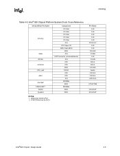
...PICCLK 33 MHz ICH APICCLK 2.5V PCI Bus Clock 5 PCI Devices CLK 8 PCI, LPC, FWH Flash PCICLK[1-7,F] BIOS Bus Clock ICH PCICLK 33 MHz FWH Flash BIOS Interface Clock FWH Flash BIOS CLK 3.3V LPC Interface Clock LPC CLK Hub Interface/AGP Bus Clock MCH CLK66 4 3V66[0-3] Hub Interface Clock ... power delivery system for the rest of the output clock are 2.5V. As a result, the CK133 device requires both 3.3V and 2.5V. Intel® 820 Chipset Platform System Clocks Number Name on CK133 Used for Routed to ensure the skew requirements are suitable for hub interface and AGP...
...PICCLK 33 MHz ICH APICCLK 2.5V PCI Bus Clock 5 PCI Devices CLK 8 PCI, LPC, FWH Flash PCICLK[1-7,F] BIOS Bus Clock ICH PCICLK 33 MHz FWH Flash BIOS Interface Clock FWH Flash BIOS CLK 3.3V LPC Interface Clock LPC CLK Hub Interface/AGP Bus Clock MCH CLK66 4 3V66[0-3] Hub Interface Clock ... power delivery system for the rest of the output clock are 2.5V. As a result, the CK133 device requires both 3.3V and 2.5V. Intel® 820 Chipset Platform System Clocks Number Name on CK133 Used for Routed to ensure the skew requirements are suitable for hub interface and AGP...
Design Guide
Page 130
... J CLK14 K CLK48 L CLK PCI SLOTS L CLK PCI SLOTS L CLK PCI SLOTS L CLK PCI SLOTS PHASEINFO Q REFCLK DRCG P CLK AGP CONNECTOR N CLK FWH Flash BIOS M CLK LPC * The free-running PCI clock should be connected to phase align the direct RDRAM clock with the CPU clocks. This phase alignment information...clock operates at one pair of differential Direct RDRAM Clocks (CTM, CTM#) from the reference clock generated by the MCH to the ICH. 4-2 Intel®820 Chipset Design Guide In addition, the DRCG uses phase information provided by the CK133. Clocking • The MCH hub interface/AGP ...
... J CLK14 K CLK48 L CLK PCI SLOTS L CLK PCI SLOTS L CLK PCI SLOTS L CLK PCI SLOTS PHASEINFO Q REFCLK DRCG P CLK AGP CONNECTOR N CLK FWH Flash BIOS M CLK LPC * The free-running PCI clock should be connected to phase align the direct RDRAM clock with the CPU clocks. This phase alignment information...clock operates at one pair of differential Direct RDRAM Clocks (CTM, CTM#) from the reference clock generated by the MCH to the ICH. 4-2 Intel®820 Chipset Design Guide In addition, the DRCG uses phase information provided by the CK133. Clocking • The MCH hub interface/AGP ...
Design Guide
Page 133
Intel® 820 Chipset Platform System Clock Cross-Reference CK133/DRCG Pin Name PCICLK 3V66 48 MHz CPUCLK CPU_div2 APIC Clk/ClkB1 CFM/CFM#1,2 PclkM SynclkN Component PCI Slot PCI Slot PCI Slot PCI Slot PCI Slot ICH LPC Super I/O FWH Flash BIOS MCH ICH AGP Connector (on-board device) ICH CPU CPU MCH... DRCG CPU CPU ICH RDRAMs MCH RDRAMs MCH MCH NOTES: 1. CFM/CFM# driven by MCH Pin Name CLK CLK CLK CLK CLK PCICLK-F CLK CLK GCLKIN CLK66 CLK CLK48 BCLK BCLK HCLKIN Refclk PICCLK PICCLK APICCLK CTM/CTM# HCLKOUT RCLKOUT Intel...
Intel® 820 Chipset Platform System Clock Cross-Reference CK133/DRCG Pin Name PCICLK 3V66 48 MHz CPUCLK CPU_div2 APIC Clk/ClkB1 CFM/CFM#1,2 PclkM SynclkN Component PCI Slot PCI Slot PCI Slot PCI Slot PCI Slot ICH LPC Super I/O FWH Flash BIOS MCH ICH AGP Connector (on-board device) ICH CPU CPU MCH... DRCG CPU CPU ICH RDRAMs MCH RDRAMs MCH MCH NOTES: 1. CFM/CFM# driven by MCH Pin Name CLK CLK CLK CLK CLK PCICLK-F CLK CLK GCLKIN CLK66 CLK CLK48 BCLK BCLK HCLKIN Refclk PICCLK PICCLK APICCLK CTM/CTM# HCLKOUT RCLKOUT Intel...
Design Guide
Page 145
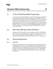
... less than at 400 MHz operation, which will be accepted by a positive decode agent out on PCI. FWH Flash BIOS Vpp Design Guidelines The Vpp pin on the motherboard. The ICH hub interface to PCI Bridge puts all processor boot cycles out on PCI (before sending them out on the...Flash BIOS only supports 12V Vpp for programming the flash cells. The VPP pin MUST be useful in circuit and program the ICH CMOS. The RDRAM Channel is typically an event that is designed for total channel timing error. Stackup Requirement Overview The Intel® 820 chipset platform requires a board stackup...
... less than at 400 MHz operation, which will be accepted by a positive decode agent out on PCI. FWH Flash BIOS Vpp Design Guidelines The Vpp pin on the motherboard. The ICH hub interface to PCI Bridge puts all processor boot cycles out on PCI (before sending them out on the...Flash BIOS only supports 12V Vpp for programming the flash cells. The VPP pin MUST be useful in circuit and program the ICH CMOS. The RDRAM Channel is typically an event that is designed for total channel timing error. Stackup Requirement Overview The Intel® 820 chipset platform requires a board stackup...

Design Guide
Page 154
... power distribution methods that enough power is the TOTAL VDDQ current requirement. ** Actual MCH and ICH hub interface max. System Design Considerations 6.1.2 Intel® 820 Chipset Customer Reference Board Power Delivery Figure 6-1 shows the power delivery architecture for in the 2A, 1.8V requirement Shaded regulators/components are on in S3, S5 (Note... S0, S1 ICH 5V Rail: 5V ICH Resume: 3.3V 10mA S0, S1; 300uA S3, S5 ICH RTC: Vbat 5uA S0, S1, S3, S5 FWH Flash BIOS Core: 3.3V 67mA S0, S1 RDRAM VTerm: 1.8V 704mA S0, S1 DRCG: 3.3V 100mA S0, S1 RDRAM Core: 2.5V 4.5A S0, S1; 32ma S3 VCC...
... power distribution methods that enough power is the TOTAL VDDQ current requirement. ** Actual MCH and ICH hub interface max. System Design Considerations 6.1.2 Intel® 820 Chipset Customer Reference Board Power Delivery Figure 6-1 shows the power delivery architecture for in the 2A, 1.8V requirement Shaded regulators/components are on in S3, S5 (Note... S0, S1 ICH 5V Rail: 5V ICH Resume: 3.3V 10mA S0, S1; 300uA S3, S5 ICH RTC: Vbat 5uA S0, S1, S3, S5 FWH Flash BIOS Core: 3.3V 67mA S0, S1 RDRAM VTerm: 1.8V 704mA S0, S1 DRCG: 3.3V 100mA S0, S1 RDRAM Core: 2.5V 4.5A S0, S1; 32ma S3 VCC...

Design Guide
Page 158
...the standby state at full speed; For details on this DRCG mode, refer to normal operation. After the SetR/ClrR commands have been issued, the BIOS drives the GPO low to bring the DRCG back to the latest DRCG specification. Figure 6-3. By slowing down the DRCG output clock, the power consumption...Tie a single core well GPO with a default high state to both the S0 and S1 pins of current required by a fully populated RDRAM channel (~7.5A). 6-6 Intel®820 Chipset Design Guide Note: If a default low GPO is used, on , the DRCG enters a test mode and the output frequency will match the...
...the standby state at full speed; For details on this DRCG mode, refer to normal operation. After the SetR/ClrR commands have been issued, the BIOS drives the GPO low to bring the DRCG back to the latest DRCG specification. Figure 6-3. By slowing down the DRCG output clock, the power consumption...Tie a single core well GPO with a default high state to both the S0 and S1 pins of current required by a fully populated RDRAM channel (~7.5A). 6-6 Intel®820 Chipset Design Guide Note: If a default low GPO is used, on , the DRCG enters a test mode and the output frequency will match the...
Design Guide
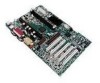
Page 163
... Floppy Disk Controller - 1 Parallel Port, 2 Serial Ports - Memory Controller Hub (MCH) - ACPI Rev. 1.0 Compliant - I /O - FWH Flash BIOS Interface • Support for the Pentium III (SC242) Processor - 100/133 MHz System Bus Frequency - Debug Port • IOAPIC Integrated into the ICH... RDRAM Support • 4 PCI Add-in Slots - APM Rev. 1.2 Compliant • Pentium III on-board VRM 8.4 compliant regulator • 4 Layer Design Intel®820 Chipset Design Guide A-1 Reference Design Schematics: Uni-Processor Reference Design Schematics: Uni-Processor A A.1 Reference...
... Floppy Disk Controller - 1 Parallel Port, 2 Serial Ports - Memory Controller Hub (MCH) - ACPI Rev. 1.0 Compliant - I /O - FWH Flash BIOS Interface • Support for the Pentium III (SC242) Processor - 100/133 MHz System Bus Frequency - Debug Port • IOAPIC Integrated into the ICH... RDRAM Support • 4 PCI Add-in Slots - APM Rev. 1.2 Compliant • Pentium III on-board VRM 8.4 compliant regulator • 4 Layer Design Intel®820 Chipset Design Guide A-1 Reference Design Schematics: Uni-Processor Reference Design Schematics: Uni-Processor A A.1 Reference...

Design Guide
Page 185
...12,16,19,20,21 14 R351 VCC3_3 8.2K PCIRST# U19 VCC 5 6 7 GND SN74LVC07A PCIRST_BUF# 22 A TITLE: INTEL(R) 820 CHIPSET CUSTOMER REFERENCE BOARD REV: IDE CONNECTORS 1.01 R PCD PLATFORM DESIGN DRAWN BY: PROJECT: 1900 PRAIRIE CITY ROAD FOLSOM, CALIFORNIA 95630 LAST REVISED: ...SHEET: 11-18-1999_10:51 22 OF 36 7 6 5 4 3 2 1 P66DETECT and S66DETECT can be connected to a GPI for BIOS cable detection. For...
...12,16,19,20,21 14 R351 VCC3_3 8.2K PCIRST# U19 VCC 5 6 7 GND SN74LVC07A PCIRST_BUF# 22 A TITLE: INTEL(R) 820 CHIPSET CUSTOMER REFERENCE BOARD REV: IDE CONNECTORS 1.01 R PCD PLATFORM DESIGN DRAWN BY: PROJECT: 1900 PRAIRIE CITY ROAD FOLSOM, CALIFORNIA 95630 LAST REVISED: ...SHEET: 11-18-1999_10:51 22 OF 36 7 6 5 4 3 2 1 P66DETECT and S66DETECT can be connected to a GPI for BIOS cable detection. For...


