Design Guide
Page 3
... 1-9 1.4.6 AC'97 1-10 1.4.7 Low Pin Count (LPC) Interface 1-11 2 Layout/Routing Guidelines 2-1 2.1 General Recommendations 2-1 2.2 Component Quadrant Layout 2-1 2.3 Intel® 820 Chipset Component Placement 2-3 2.4 Core Chipset Routing Recommendations 2-4 2.5 Source Synchronous Strobing 2-5 2.6 Direct Rambus* Interface 2-7 2.6.1 Stackup 2-8 2.6.2 Direct Rambus*...and 4X 2-39 2.7.9 Compensation 2-41 2.7.10 AGP Pull-ups 2-41 2.7.11 Motherboard / Add-in Card Interoperability 2-42 2.8 Hub Interface 2-43 2.8.1 Data Signals 2-44 2.8.2 Strobe Signals 2-44 2.8.3 ...
... 1-9 1.4.6 AC'97 1-10 1.4.7 Low Pin Count (LPC) Interface 1-11 2 Layout/Routing Guidelines 2-1 2.1 General Recommendations 2-1 2.2 Component Quadrant Layout 2-1 2.3 Intel® 820 Chipset Component Placement 2-3 2.4 Core Chipset Routing Recommendations 2-4 2.5 Source Synchronous Strobing 2-5 2.6 Direct Rambus* Interface 2-7 2.6.1 Stackup 2-8 2.6.2 Direct Rambus*...and 4X 2-39 2.7.9 Compensation 2-41 2.7.10 AGP Pull-ups 2-41 2.7.11 Motherboard / Add-in Card Interoperability 2-42 2.8 Hub Interface 2-43 2.8.1 Data Signals 2-44 2.8.2 Strobe Signals 2-44 2.8.3 ...
Design Guide
Page 4
...60 2.14 AC'97 ...2-61 2.14.1 AC'97 Signal Quality Requirements 2-63 2.14.2 AC'97 Motherboard Implementation 2-63 2.15 USB ...2-65 2.16 ISA (82380AB 2-66 2.16.1 ICH GPIO connected to 82380AB...3-4 3.2.1 Initial Timing Analysis 3-5 3.2.2 Determine General Topology, Layout, and Routing Desired ...........3-8 3.2.3 Pre-Layout Simulation 3-8 3.2.4 Place and Route Board 3-10 3.2.5 Post-Layout Simulation 3-13 3.2.6 Validation 3-14 3.3 Theory...3-15 3.3.1 AGTL 3-15 3.3.2 Timing Requirements 3-16 3.3.3 Cross-talk Theory... 3-20 3.4.4 Clock Routing 3-23 iv Intel® 820 Chipset Design Guide
...60 2.14 AC'97 ...2-61 2.14.1 AC'97 Signal Quality Requirements 2-63 2.14.2 AC'97 Motherboard Implementation 2-63 2.15 USB ...2-65 2.16 ISA (82380AB 2-66 2.16.1 ICH GPIO connected to 82380AB...3-4 3.2.1 Initial Timing Analysis 3-5 3.2.2 Determine General Topology, Layout, and Routing Desired ...........3-8 3.2.3 Pre-Layout Simulation 3-8 3.2.4 Place and Route Board 3-10 3.2.5 Post-Layout Simulation 3-13 3.2.6 Validation 3-14 3.3 Theory...3-15 3.3.1 AGTL 3-15 3.3.2 Timing Requirements 3-16 3.3.3 Cross-talk Theory... 3-20 3.4.4 Clock Routing 3-23 iv Intel® 820 Chipset Design Guide
Design Guide
Page 6
... generated Hub Interface Reference Dividers 2-45 Intel® Pentium® III Processor Dual Processor Configuration 2-46 Intel® Pentium® III Processor Uni-Processor Configuration 2-46 Ground Plane Reference (Four Layer Motherboard 2-47 Hole Locations and Keepout Zones ...37 2-38 2-39 2-40 2-41 2-42 2-43 Intel® 820 Chipset Platform Performance Desktop Block Diagram 1-5 Intel® 820 Chipset Platform Performance Desktop Block Diagram (with ISA Bridge 1-6 Intel® 820 Chipset Platform Dual-Processor Performance Desktop Block Diagram 1-7 AC'97 Connections 1-11 MCH 324-...
... generated Hub Interface Reference Dividers 2-45 Intel® Pentium® III Processor Dual Processor Configuration 2-46 Intel® Pentium® III Processor Uni-Processor Configuration 2-46 Ground Plane Reference (Four Layer Motherboard 2-47 Hole Locations and Keepout Zones ...37 2-38 2-39 2-40 2-41 2-42 2-43 Intel® 820 Chipset Platform Performance Desktop Block Diagram 1-5 Intel® 820 Chipset Platform Performance Desktop Block Diagram (with ISA Bridge 1-6 Intel® 820 Chipset Platform Dual-Processor Performance Desktop Block Diagram 1-7 AC'97 Connections 1-11 MCH 324-...
Design Guide
Page 8
... TFLT_MIN Calculations (Frequency Independent 3-8 Trace Width Space Guidelines 3-11 Host Clock Routing 3-12 Intel® 820 Chipset Platform System Clocks 4-1 Intel® 820 Chipset Platform Clock Skews 4-3 Intel® 820 Chipset Platform System Clock Cross-Reference 4-5 Placement Guidelines for Motherboard Routing Lengths 4-8 External DRCG Component Values 4-10 Unused Output Termination 4-12 DRCG Ratio 4-12...
... TFLT_MIN Calculations (Frequency Independent 3-8 Trace Width Space Guidelines 3-11 Host Clock Routing 3-12 Intel® 820 Chipset Platform System Clocks 4-1 Intel® 820 Chipset Platform Clock Skews 4-3 Intel® 820 Chipset Platform System Clock Cross-Reference 4-5 Placement Guidelines for Motherboard Routing Lengths 4-8 External DRCG Component Values 4-10 Unused Output Termination 4-12 DRCG Ratio 4-12...
Design Guide
Page 13
... Considerations"- This chapter also provides an overview of the Intel® 820 chipset. • Chapter 2, "Layout/Routing Guidelines"-This chapter provides a detailed set of schematics for board designers while reducing the risk of motherboard layout and routing guidelines for board designers. This appendix provides a set of board-related issues. The guidelines have been developed to...
... Considerations"- This chapter also provides an overview of the Intel® 820 chipset. • Chapter 2, "Layout/Routing Guidelines"-This chapter provides a detailed set of schematics for board designers while reducing the risk of motherboard layout and routing guidelines for board designers. This appendix provides a set of board-related issues. The guidelines have been developed to...
Design Guide
Page 27
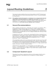
... mil spaces must be used to conduct routing analysis. Layout/Routing Guidelines Layout/Routing Guidelines 2 This chapter documents motherboard layout and routing guidelines for Intel® 820 chipset based systems. This section does not discuss the functional aspects of any bus, or the ... to consider the minimum and maximum impedance of neighboring traces. In addition, the PCB should be fabricated as documented in neighboring traces. Intel®820 Chipset Design Guide 2-1 If this section (except where noted) assume 5 mil wide traces. Caution: If the guidelines listed...
... mil spaces must be used to conduct routing analysis. Layout/Routing Guidelines Layout/Routing Guidelines 2 This chapter documents motherboard layout and routing guidelines for Intel® 820 chipset based systems. This section does not discuss the functional aspects of any bus, or the ... to consider the minimum and maximum impedance of neighboring traces. In addition, the PCB should be fabricated as documented in neighboring traces. Intel®820 Chipset Design Guide 2-1 If this section (except where noted) assume 5 mil wide traces. Caution: If the guidelines listed...
Design Guide
Page 35
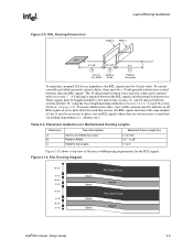
...10 mils 6 mils 18 mils 6 mils 10 mils 6 mils Space Space Space Space RSL Signal Trace Ground RSL Signal Trace Ground Intel®820 Chipset Design Guide 2-9 The 10 mil ground isolation traces must be a 10 mil ground isolation trace routed between the RSL...C RIMM to Termination 0" to 3.50" 0.4" - 0.45" 0" to meet this via every 1". Layout/Routing Guidelines Figure 2-9. Placement Guidelines for Motherboard Routing Lengths Reference Trace Description Maximum Trace Length (in Section 2.6.2.6, "Length Matching Methods" on all RSL signals at every neck-down for the RSL signals...
...10 mils 6 mils 18 mils 6 mils 10 mils 6 mils Space Space Space Space RSL Signal Trace Ground RSL Signal Trace Ground Intel®820 Chipset Design Guide 2-9 The 10 mil ground isolation traces must be a 10 mil ground isolation trace routed between the RSL...C RIMM to Termination 0" to 3.50" 0.4" - 0.45" 0" to meet this via every 1". Layout/Routing Guidelines Figure 2-9. Placement Guidelines for Motherboard Routing Lengths Reference Trace Description Maximum Trace Length (in Section 2.6.2.6, "Length Matching Methods" on all RSL signals at every neck-down for the RSL signals...
Design Guide
Page 40
...Equation is an approximation that can be used for the recommended stackup was determined through simulation. Table 2-3 shows example copper tab areas. 2-14 Intel®820 Chipset Design Guide Based on the stackup requirement in mils of the layer on page 5-1 the copper tab area should be on... the Direct Rambus* channel. The copper tab area for calculating copper tab area on the motherboard by adding a copper tab to the specified RSL pins at each connector: LCTM RCTM LCFM RCFM LROW[2:0] LCOL[4:0] RDQA[8:0] RDQB[8:0] SCK LCTM# ...
...Equation is an approximation that can be used for the recommended stackup was determined through simulation. Table 2-3 shows example copper tab areas. 2-14 Intel®820 Chipset Design Guide Based on the stackup requirement in mils of the layer on page 5-1 the copper tab area should be on... the Direct Rambus* channel. The copper tab area for calculating copper tab area on the motherboard by adding a copper tab to the specified RSL pins at each connector: LCTM RCTM LCFM RCFM LROW[2:0] LCOL[4:0] RDQA[8:0] RDQB[8:0] SCK LCTM# ...
Design Guide
Page 49
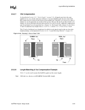
... 2000 mils was chosen as documented in Section 2.8.2, "Strobe Signals" on page 2-44, all signals that are the correct length. Intel®820 Chipset Design Guide 2-23 Because the electrical characteristics of a dummy via do not match the electrical characteristics of additional trace ... vs. Each signal with a dummy via + 25 mils of vias. Therefore, it is : a real via = a dummy via must have 25 mils of the motherboard. Real "Via" "DUMMY Via" Trace "REAL Via" Trace PCB PCB PCB PCB Via Via Trace 2.6.2.8 Length Matching & Via Compensation Example Table 2-5 can be routed ...
... 2000 mils was chosen as documented in Section 2.8.2, "Strobe Signals" on page 2-44, all signals that are the correct length. Intel®820 Chipset Design Guide 2-23 Because the electrical characteristics of a dummy via do not match the electrical characteristics of additional trace ... vs. Each signal with a dummy via + 25 mils of vias. Therefore, it is : a real via = a dummy via must have 25 mils of the motherboard. Real "Via" "DUMMY Via" Trace "REAL Via" Trace PCB PCB PCB PCB Via Via Trace 2.6.2.8 Length Matching & Via Compensation Example Table 2-5 can be routed ...
Design Guide
Page 50
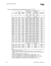
...Motherboard Trace = (Nominal RSL Length - Formula A max: Motherboard Trace = (Nominal RSL Length - Package Dimension) + 10 mil 7. Line Matching and Via Compensation Example1,2,3,4,5,6,7,8,9,10 Signal Ball on MCH Nominal RSL Length (mils) Package Dimension (mils) Motherboard... Trace Length when Routed on Bottom (i.e., Real Via) Min (mils) Max (mils) Motherboard...Motherboard Trace = (Nominal RSL Length - Package Dimension) - 10 mil + 25 mil 8. Package Dimension) * 1.021 10.Formula D: Motherboard...side of the motherboard; 2. Formula B min: Motherboard Trace = (...
...Motherboard Trace = (Nominal RSL Length - Formula A max: Motherboard Trace = (Nominal RSL Length - Package Dimension) + 10 mil 7. Line Matching and Via Compensation Example1,2,3,4,5,6,7,8,9,10 Signal Ball on MCH Nominal RSL Length (mils) Package Dimension (mils) Motherboard... Trace Length when Routed on Bottom (i.e., Real Via) Min (mils) Max (mils) Motherboard...Motherboard Trace = (Nominal RSL Length - Package Dimension) - 10 mil + 25 mil 8. Package Dimension) * 1.021 10.Formula D: Motherboard...side of the motherboard; 2. Formula B min: Motherboard Trace = (...

Design Guide
Page 52
...SIO signal must be shunted to the MCH (i.e., it will be accomplished using the NPN transistor shown in circuit shown in Figure 2-17. The motherboard routing lengths for the SIO signal are the same as shown in Figure 2-28. Figure 2-27. To avoid the MCH inadvertently taking the ...to match the electrical characteristics on the SOUT pin of the MCH outputs is entering and exiting Suspend-to ground (i.e., always turned off). 2-26 Intel®820 Chipset Design Guide This shunting can be powering-up or powering-down). This transistor's base should have a Cobo of the commands (the...
...SIO signal must be shunted to the MCH (i.e., it will be accomplished using the NPN transistor shown in circuit shown in Figure 2-17. The motherboard routing lengths for the SIO signal are the same as shown in Figure 2-28. Figure 2-27. To avoid the MCH inadvertently taking the ...to match the electrical characteristics on the SOUT pin of the MCH outputs is entering and exiting Suspend-to ground (i.e., always turned off). 2-26 Intel®820 Chipset Design Guide This shunting can be powering-up or powering-down). This transistor's base should have a Cobo of the commands (the...
Design Guide
Page 54
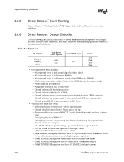
... example) - Via to the ground pins in the middle of the MCH edge and the connector edge - Ground island (for Intel® 820 chipset platform Direct Rambus* clock routing guidelines. 2.6.6 Direct Rambus* Design Checklist Use the following checklist as a final check to ... (Aluminum/Electrolytic capacitors are near high-frequency capacitors - 100uF TANTALUM capacitors should NOT have AT LEAST 2 vias/cap to ensure the motherboard incorporates solid design practices. No unconnected ground floods - All ground isolation at each end of isolation island - Ground pins in the ...
... example) - Via to the ground pins in the middle of the MCH edge and the connector edge - Ground island (for Intel® 820 chipset platform Direct Rambus* clock routing guidelines. 2.6.6 Direct Rambus* Design Checklist Use the following checklist as a final check to ... (Aluminum/Electrolytic capacitors are near high-frequency capacitors - 100uF TANTALUM capacitors should NOT have AT LEAST 2 vias/cap to ensure the motherboard incorporates solid design practices. No unconnected ground floods - All ground isolation at each end of isolation island - Ground pins in the ...

Design Guide
Page 56
...the MB will have a "dummy via " while signals routed on each side of the motherboard. When clock signals serpentine, they are routed on the secondary side of the differential pair. 2-30 Intel®820 Chipset Design Guide If signals are routed on the primary side of the Vterm... must be length compensated (using the 1.021 length factor described in the following table. In these signals AND include the ground side of the motherboard. - This includes all signals with a dummy via near high-speed signals • RSL Routing - At least 10 mils ground flood isolation ...
...the MB will have a "dummy via " while signals routed on each side of the motherboard. When clock signals serpentine, they are routed on the secondary side of the differential pair. 2-30 Intel®820 Chipset Design Guide If signals are routed on the primary side of the Vterm... must be length compensated (using the 1.021 length factor described in the following table. In these signals AND include the ground side of the motherboard. - This includes all signals with a dummy via near high-speed signals • RSL Routing - At least 10 mils ground flood isolation ...
Design Guide
Page 59
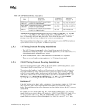
...the routing rules used on rising clock edges. All data is used in 1X mode. When the term data is sampled on the motherboard. The maximum line length and length mismatch requirements are not used , it is referring to one of the signals listed as 1X...long. Guidelines for short AGP interfaces (e.g., < 6") and the long AGP interfaces (e.g., > 6" and < 7.25") are for 2X/4X lines (data and strobes). Intel®820 Chipset Design Guide 2-33 These guidelines are documented separately. AGP 2.0 Data/Strobe Associations Data Associated Strobe in 1X AD[15:0] and Strobes are...
...the routing rules used on rising clock edges. All data is used in 1X mode. When the term data is sampled on the motherboard. The maximum line length and length mismatch requirements are not used , it is referring to one of the signals listed as 1X...long. Guidelines for short AGP interfaces (e.g., < 6") and the long AGP interfaces (e.g., > 6" and < 7.25") are for 2X/4X lines (data and strobes). Intel®820 Chipset Design Guide 2-33 These guidelines are documented separately. AGP 2.0 Data/Strobe Associations Data Associated Strobe in 1X AD[15:0] and Strobes are...
Design Guide
Page 62
...possible to the MCH and/or close to minimize signal integrity problems on the motherboard, add-in the switching range. The narrowing of the via field as possible (1" maximum). 2-36 Intel®820 Chipset Design Guide Recommendations Decoupling • For VDDQ decoupling, a ...minimum of six (6) 0.01 uF capacitors are recommended for as short a distance as possible. • Ensure that the motherboard is allotted 0.9 ns of the board to another. This 1...
...possible to the MCH and/or close to minimize signal integrity problems on the motherboard, add-in the switching range. The narrowing of the via field as possible (1" maximum). 2-36 Intel®820 Chipset Design Guide Recommendations Decoupling • For VDDQ decoupling, a ...minimum of six (6) 0.01 uF capacitors are recommended for as short a distance as possible. • Ensure that the motherboard is allotted 0.9 ns of the board to another. This 1...
Design Guide
Page 63
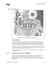
...the MCH to an AGP connector (or to an AGP video controller if implemented as both are tied to the 3.3V power plane on board layout. Figure 2-30. The recommendations above , it is strongly recommended that half of vias on each net; Top Signal Layer Layout/...signals be reference to ground. An ideal design would have the complete AGP interface signal field referenced to ground depending on the motherboard. VCC is always 3.3V. Intel®820 Chipset Design Guide 2-37 VDDQ Generation and TYPEDET# AGP specifies two separate power planes (VCC and VDDQ). AD_STB0,...
...the MCH to an AGP connector (or to an AGP video controller if implemented as both are tied to the 3.3V power plane on board layout. Figure 2-30. The recommendations above , it is strongly recommended that half of vias on each net; Top Signal Layer Layout/...signals be reference to ground. An ideal design would have the complete AGP interface signal field referenced to ground depending on the motherboard. VCC is always 3.3V. Intel®820 Chipset Design Guide 2-37 VDDQ Generation and TYPEDET# AGP specifies two separate power planes (VCC and VDDQ). AD_STB0,...
Design Guide
Page 64
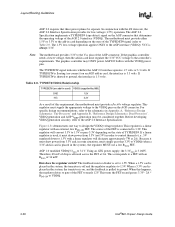
...divider is always 3.3V. When a 3.3V card is placed in the system, the transistor is allowed across the FET at 2A). When this requirement, the motherboard must supply the appropriate voltage to 3.1V. The AGP 2.0 Specification implements a TYPEDET# (type detect) signal on , and the feedback is 3.168V. Table... AGP add-in order to control thermals (i.e., 5V regulated down to the Vcc pins of 34 mW. The motherboard must regulate the 3.3V VCC voltage to VDDQ. 2-38 Intel®820 Chipset Design Guide This corresponds to Table 2-9. Because it must draw power from 3.3V and, in...
...divider is always 3.3V. When a 3.3V card is placed in the system, the transistor is allowed across the FET at 2A). When this requirement, the motherboard must supply the appropriate voltage to 3.1V. The AGP 2.0 Specification implements a TYPEDET# (type detect) signal on , and the feedback is 3.168V. Table... AGP add-in order to control thermals (i.e., 5V regulated down to the Vcc pins of 34 mW. The motherboard must regulate the 3.3V VCC voltage to VDDQ. 2-38 Intel®820 Chipset Design Guide This corresponds to Table 2-9. Because it must draw power from 3.3V and, in...
Design Guide
Page 65
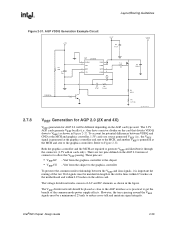
... pins are two pins defined on the card that divides VDDQ down to the strobe lines within 0.5 inches on the motherboard and within 0.25 inches on the AGP card type used. Intel®820 Chipset Design Guide 2-39 Refer to the graphics controller). Both the graphics controller and the MCH are required...
... pins are two pins defined on the card that divides VDDQ down to the strobe lines within 0.5 inches on the motherboard and within 0.25 inches on the AGP card type used. Intel®820 Chipset Design Guide 2-39 Refer to the graphics controller). Both the graphics controller and the MCH are required...

Design Guide
Page 67
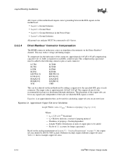
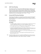
Layout/Routing Guidelines 2.7.9 2.7.10 Compensation The MCH AGP interface supports resistive buffer compensation (RCOMP). Tie the GRCOMP pin to a 40 Ω 2% (or 39 Ω 1%) pull-down resistor (to ground) via a 10 mil wide, very short (
Layout/Routing Guidelines 2.7.9 2.7.10 Compensation The MCH AGP interface supports resistive buffer compensation (RCOMP). Tie the GRCOMP pin to a 40 Ω 2% (or 39 Ω 1%) pull-down resistor (to ground) via a 10 mil wide, very short (
Design Guide
Page 68
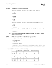
... AGP interface are in the VDDQ group. Voltage/Data Rate Interoperability 1X 2X 4X 1.5V VDDQ Yes Yes Yes 3.3V VDDQ Yes Yes No 2-42 Intel®820 Chipset Design Guide They are not 3.3V tolerant during 1.5V operation: • PME# • INTA# • INTB# • GPERR#...2.7.10.1 AGP Signal Voltage Tolerance List The following signals on the AGP interface are 3.3V tolerant during 1.5V AGP operation. 2.7.11 Motherboard / Add-in Card Interoperability Currently, there are three AGP connectors: • 3.3V AGP connector • 1.5V AGP connector • Universal AGP connector...
... AGP interface are in the VDDQ group. Voltage/Data Rate Interoperability 1X 2X 4X 1.5V VDDQ Yes Yes Yes 3.3V VDDQ Yes Yes No 2-42 Intel®820 Chipset Design Guide They are not 3.3V tolerant during 1.5V operation: • PME# • INTA# • INTB# • GPERR#...2.7.10.1 AGP Signal Voltage Tolerance List The following signals on the AGP interface are 3.3V tolerant during 1.5V AGP operation. 2.7.11 Motherboard / Add-in Card Interoperability Currently, there are three AGP connectors: • 3.3V AGP connector • 1.5V AGP connector • Universal AGP connector...


