
MANUAL
Page 3
...; Technology (EIST). Supports Intel Pentium 4 processor and Celeron D. Supports Dual Core CPU Supports Pentium D Supports Core2Duo (For Ver 2.0 only) Front Side Bus at the following frequency ranges: 533MT/s (133MHzCore Clock) 800MT/s (200MHzCore Clock) ... (Intel EM64T). Supports Execute Disable Bit Technology (XD). Chipset North Bridge: Intel 945P South Bridge: Intel ICH7. IDE 1 on-board connectors support 2 IDE disk drives. Biostar T-Series TForce 945P CHAPTER 1: INTRODUCTION 1.1 MOTHERBOARD FEATURES CPU Supports LGA 775. Supports PIO mode 0-4, ...
...; Technology (EIST). Supports Intel Pentium 4 processor and Celeron D. Supports Dual Core CPU Supports Pentium D Supports Core2Duo (For Ver 2.0 only) Front Side Bus at the following frequency ranges: 533MT/s (133MHzCore Clock) 800MT/s (200MHzCore Clock) ... (Intel EM64T). Supports Execute Disable Bit Technology (XD). Chipset North Bridge: Intel 945P South Bridge: Intel ICH7. IDE 1 on-board connectors support 2 IDE disk drives. Biostar T-Series TForce 945P CHAPTER 1: INTRODUCTION 1.1 MOTHERBOARD FEATURES CPU Supports LGA 775. Supports PIO mode 0-4, ...
MANUAL
Page 5
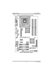
SATA4 IR JPANEL1 (optional ) 3 User's Manual Biostar T-Series TForce 945P 1.2 LAYOUT AND COMPONENTS (VER 1.X) JKBMS1 JKBV1 LGA775 COJMC1OM1 CPU1 JPRNT1 DDR2_A1 DDR2_A2 DDR2_B1 DDR2_B2 JUSB2 JRJ45USB1 JATXPWR2 JCFAN1 Intel 945P JAUDIO1 JAUDIO6 JCDIN1 Codec JATXPWR1 PCI-Ex16 JDDR2_OV_3V Super I/O PCI-Ex1_1 PCI-Ex1_2 BAT1 Intel ICH7 IDE1 BIOS PCI1 PCI2 SATA1 SATA3 JCI1 10/100 LAN PCI3 JSFAN1 JCMOS1 SATA2 JUSB3 JUSB4 FDD1 JSPDIF_OUT1 Note: ■ represents the 1st pin.
SATA4 IR JPANEL1 (optional ) 3 User's Manual Biostar T-Series TForce 945P 1.2 LAYOUT AND COMPONENTS (VER 1.X) JKBMS1 JKBV1 LGA775 COJMC1OM1 CPU1 JPRNT1 DDR2_A1 DDR2_A2 DDR2_B1 DDR2_B2 JUSB2 JRJ45USB1 JATXPWR2 JCFAN1 Intel 945P JAUDIO1 JAUDIO6 JCDIN1 Codec JATXPWR1 PCI-Ex16 JDDR2_OV_3V Super I/O PCI-Ex1_1 PCI-Ex1_2 BAT1 Intel ICH7 IDE1 BIOS PCI1 PCI2 SATA1 SATA3 JCI1 10/100 LAN PCI3 JSFAN1 JCMOS1 SATA2 JUSB3 JUSB4 FDD1 JSPDIF_OUT1 Note: ■ represents the 1st pin.

MANUAL
Page 6
Biostar T-Series TForce 945P 1.3 LAYOUT AND COMPONENTS (VER 2.X) JKBMS1 JKBV1 LGA775 COJMC1OM1 CPU1 JPRNT1 DDR2_A1 DDR2_A2 DDR2_B1 DDR2_B2 JUSB2 JRJ45USB1 JATXPWR2 JCFAN1 Intel 945P JAUDIO1 JAUDIO6 JCDIN1 Codec JATXPWR1 PCI-Ex16 JDDRII_2.2V Super I/O PCI-Ex1_1 PCI-Ex1_2 BAT1 Intel ICH7 IDE1 BIOS PCI1 PCI2 SATA1 SATA3 JCI1 10/100 LAN PCI3 JSFAN1 JCMOS1 SATA2 JUSB3 JUSB4 FDD1 JSPDIF_OUT1 Note: ■ represents the 1st pin. SATA4 RSTSW1 JPANEL1 PWRSW1 4 User's Manual
Biostar T-Series TForce 945P 1.3 LAYOUT AND COMPONENTS (VER 2.X) JKBMS1 JKBV1 LGA775 COJMC1OM1 CPU1 JPRNT1 DDR2_A1 DDR2_A2 DDR2_B1 DDR2_B2 JUSB2 JRJ45USB1 JATXPWR2 JCFAN1 Intel 945P JAUDIO1 JAUDIO6 JCDIN1 Codec JATXPWR1 PCI-Ex16 JDDRII_2.2V Super I/O PCI-Ex1_1 PCI-Ex1_2 BAT1 Intel ICH7 IDE1 BIOS PCI1 PCI2 SATA1 SATA3 JCI1 10/100 LAN PCI3 JSFAN1 JCMOS1 SATA2 JUSB3 JUSB4 FDD1 JSPDIF_OUT1 Note: ■ represents the 1st pin. SATA4 RSTSW1 JPANEL1 PWRSW1 4 User's Manual
MANUAL
Page 18
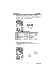
Pin Assignment 1 +5V 2 SPDIF OUT 3 Ground 31 16 User's Manual Biostar T-Series TForce 945P JPANEL1: Header for Front Panel Facilities (Ver 2.0 only) This 16-pin connector includes Power-on button Digital Audio-out Connector: JSPDIF_OUT1 This connector allows users to connect the PC case's front panel ...
Pin Assignment 1 +5V 2 SPDIF OUT 3 Ground 31 16 User's Manual Biostar T-Series TForce 945P JPANEL1: Header for Front Panel Facilities (Ver 2.0 only) This 16-pin connector includes Power-on button Digital Audio-out Connector: JSPDIF_OUT1 This connector allows users to connect the PC case's front panel ...

MANUAL
Page 21
Biostar T-Series TForce 945P Header for Memory Voltage Customize: JDDR = 2.3V (JDDRII_2.2V in Ver 2.0) When processing Memory Voltage Overclocking, please place the jumper to 2.3V. (Consult your DDR memory module supplier) On-board buttons (Ver 2.0 only) There are 2 on-board buttons PWRSW1 RSTSW1 PWRSW1: This is an on Pin 1-2, memory voltage will be fixed at...
Biostar T-Series TForce 945P Header for Memory Voltage Customize: JDDR = 2.3V (JDDRII_2.2V in Ver 2.0) When processing Memory Voltage Overclocking, please place the jumper to 2.3V. (Consult your DDR memory module supplier) On-board buttons (Ver 2.0 only) There are 2 on-board buttons PWRSW1 RSTSW1 PWRSW1: This is an on Pin 1-2, memory voltage will be fixed at...


