
M7NCG 400 user's manual
Page 1
...instructions, may cause harmful interference to radio communications. All the brand and product names are under continual improvement, we have taken every care in whole, is the intellectual property of the vendor. This equipment generates, uses and can radiate radio frequency energy and, if not installed and used in a residential installation. M7NCG 400...user's manual, no guarantee is no representations or warranties with the limits of a Class B digital device, pursuant to make changes without notice. There is given as to the correctness of this publication and to Part...
...instructions, may cause harmful interference to radio communications. All the brand and product names are under continual improvement, we have taken every care in whole, is the intellectual property of the vendor. This equipment generates, uses and can radiate radio frequency energy and, if not installed and used in a residential installation. M7NCG 400...user's manual, no guarantee is no representations or warranties with the limits of a Class B digital device, pursuant to make changes without notice. There is given as to the correctness of this publication and to Part...
M7NCG 400 user's manual
Page 3
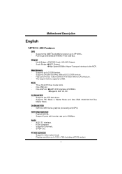
...+. - Supports four IDE disk drives. - Support s-video output mode - MMootthheerrbbooaarrdd DDeessccrriippttiioonn English M7NCG 400 Features CPU - Audio - Supports 200/266/333 MHz (without ECC) DDR devices. - One AGP slot: AGP3.0 8X interface at 200/266/333/400MHz Front Side Bus. Supports AGP 4X, 8X. Support 2 ports with transfer rate up to the MCP. High performance 128-bit DDR333 Twin Bank Memory Architecture. - Supports 6 channels. - Main Memory - PC99 complaint. - The largest memory capacity is 3GB. GeForce 4MX Series graphics...
...+. - Supports four IDE disk drives. - Support s-video output mode - MMootthheerrbbooaarrdd DDeessccrriippttiioonn English M7NCG 400 Features CPU - Audio - Supports 200/266/333 MHz (without ECC) DDR devices. - One AGP slot: AGP3.0 8X interface at 200/266/333/400MHz Front Side Bus. Supports AGP 4X, 8X. Support 2 ports with transfer rate up to the MCP. High performance 128-bit DDR333 Twin Bank Memory Architecture. - Supports 6 channels. - Main Memory - PC99 complaint. - The largest memory capacity is 3GB. GeForce 4MX Series graphics...
M7NCG 400 user's manual
Page 4
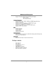
AWARD legal Bios. - HDD Cable X 1 - SPDIF OUT Cable X1 (optional) - Supports PS/2 mouse and PS/2 keyboard. - Micro ATX Form Factor: 24.4cm X 24.4cm (W X L) Package contents - User Manual X 1 - Supports 2 back USB2.0 ports and 4 front USB2.0 ports. - Supports 360K, 720K, 1.2MB, 1.44MB and 2.88MB floppy disk drivers. - Supports ACPI. - Operating System - Supports S/PDIF Out connector. Supports 2 serial ports. - USB Cable X 2 (optional) - Supports USB Function. FDD Cable X 1 - Supports APM1.2. - Offers the highest performance for MS-DOS, Windows 2000, ...
AWARD legal Bios. - HDD Cable X 1 - SPDIF OUT Cable X1 (optional) - Supports PS/2 mouse and PS/2 keyboard. - Micro ATX Form Factor: 24.4cm X 24.4cm (W X L) Package contents - User Manual X 1 - Supports 2 back USB2.0 ports and 4 front USB2.0 ports. - Supports 360K, 720K, 1.2MB, 1.44MB and 2.88MB floppy disk drivers. - Supports ACPI. - Operating System - Supports S/PDIF Out connector. Supports 2 serial ports. - USB Cable X 2 (optional) - Supports USB Function. FDD Cable X 1 - Supports APM1.2. - Offers the highest performance for MS-DOS, Windows 2000, ...
M7NCG 400 user's manual
Page 5
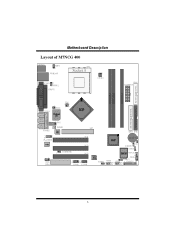
... Lan Chip 9 1 10 2 IGP PCI1 Codec 1 1 J_CODECSEL PCI2 PCI3 9 19 1 10 210 2 J1394A J1394B IDE2 IDE1 1394A Chip (optional) MCP BAT1 1 1 JC1 J_SPDIF1 JCMOS 1 BIOS JSFAN1 1 JWOL1 JUSBV1 1 JUSBV4 JUSB1 2 10 2 JUSB2 10 2 JPANEL1 1 24 11 91 91 23 SECONDARY IDE CONN. PRIMARY IDE CONN. 3 MMootthheerrbbooaarrdd DDeessccrriippttiioonn Layout of M7NCG 400 JKBMS1 JKBV1 1 JUSBLAN1 JCOM1 1 JUSBV2 JPRNT1 1 JCFAN1 FDD1 JATXPWER1 FLOPPY DISK...
... Lan Chip 9 1 10 2 IGP PCI1 Codec 1 1 J_CODECSEL PCI2 PCI3 9 19 1 10 210 2 J1394A J1394B IDE2 IDE1 1394A Chip (optional) MCP BAT1 1 1 JC1 J_SPDIF1 JCMOS 1 BIOS JSFAN1 1 JWOL1 JUSBV1 1 JUSBV4 JUSB1 2 10 2 JUSB2 10 2 JPANEL1 1 24 11 91 91 23 SECONDARY IDE CONN. PRIMARY IDE CONN. 3 MMootthheerrbbooaarrdd DDeessccrriippttiioonn Layout of M7NCG 400 JKBMS1 JKBV1 1 JUSBLAN1 JCOM1 1 JUSBV2 JPRNT1 1 JCFAN1 FDD1 JATXPWER1 FLOPPY DISK...
M7NCG 400 user's manual
Page 6
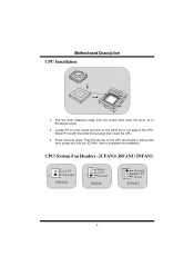
MMootthheerrbbooaarrdd DDeessccrriippttiioonn CPU Installation CPU 1. Locate Pin A in the CPU. CPU/ System Fan Headers: JCFAN1/ JSFAN1/ JNFAN1 12V 1 Ground JNFAN1 1 Ground 12V Sense JCFAN1 4 Then Put the fan on the CPU and buckle it and put the fan's power port into the JCFAN1, then to 90-degree angle. 2. Match Pin A with the white dot/cut edge in the socket and lock for the white dot or cut edge then insert the CPU. 3. Press the lever down. Pull the lever sideways away from the socket then raise the lever up to complete the installation.
MMootthheerrbbooaarrdd DDeessccrriippttiioonn CPU Installation CPU 1. Locate Pin A in the CPU. CPU/ System Fan Headers: JCFAN1/ JSFAN1/ JNFAN1 12V 1 Ground JNFAN1 1 Ground 12V Sense JCFAN1 4 Then Put the fan on the CPU and buckle it and put the fan's power port into the JCFAN1, then to 90-degree angle. 2. Match Pin A with the white dot/cut edge in the socket and lock for the white dot or cut edge then insert the CPU. 3. Press the lever down. Pull the lever sideways away from the socket then raise the lever up to complete the installation.
M7NCG 400 user's manual
Page 7
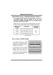
...DRAM Type: 64MB/ 128MB/ 256MB/ 512MB/ 1GB DIMM Module (184 pin) DIMM Socket Location DDR Module Total Memory Size (MB) DIMMB1 DIMMB2 DIMMA1 64MB/128MB/256MB/512MB/1GB *1 64MB/128MB/256MB/512MB/1GB *1 64MB/128MB/256MB/512MB/1GB *1 ~~~only for reference~~~ Max is 3GB How to be installed. (It has to install... DDR DIMM Modules: DIMMB1/DIMMB2/ DIMMA1 For Dual-channel DDR (128-bit) high performance, at 64-bit. The DIMM socket has a " Plastic Safety Tab", and the DIMM memory module has an "Asymmetrical notch", so the DIMM memory module can only fit into the place. 3....
...DRAM Type: 64MB/ 128MB/ 256MB/ 512MB/ 1GB DIMM Module (184 pin) DIMM Socket Location DDR Module Total Memory Size (MB) DIMMB1 DIMMB2 DIMMA1 64MB/128MB/256MB/512MB/1GB *1 64MB/128MB/256MB/512MB/1GB *1 64MB/128MB/256MB/512MB/1GB *1 ~~~only for reference~~~ Max is 3GB How to be installed. (It has to install... DDR DIMM Modules: DIMMB1/DIMMB2/ DIMMA1 For Dual-channel DDR (128-bit) high performance, at 64-bit. The DIMM socket has a " Plastic Safety Tab", and the DIMM memory module has an "Asymmetrical notch", so the DIMM memory module can only fit into the place. 3....
M7NCG 400 user's manual
Page 8
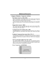
... Graphics Port (AGP). It has two HDD connectors IDE1 (primary) and IDE2 (secondary). MMootthheerrbbooaarrdd DDeessccrriippttiioonn Jumpers, Headers, Connectors & Slots Hard Disk Connectors: IDE1/ IDE2 The motherboard has a 32-bit Enhanced PCI IDE Controller that video card. Floppy Disk Connector: FDD1 The motherboard provides a standard floppy disk connector that supports 360K, 720K, 1.2M, 1.44M and 2.88M floppy disk types. This PCI slot is an open Industry Standard Architecture, and it defines a hardware scalable riser card interface, which has, supplanted the older ISA bus...
... Graphics Port (AGP). It has two HDD connectors IDE1 (primary) and IDE2 (secondary). MMootthheerrbbooaarrdd DDeessccrriippttiioonn Jumpers, Headers, Connectors & Slots Hard Disk Connectors: IDE1/ IDE2 The motherboard has a 32-bit Enhanced PCI IDE Controller that video card. Floppy Disk Connector: FDD1 The motherboard provides a standard floppy disk connector that supports 360K, 720K, 1.2M, 1.44M and 2.88M floppy disk types. This PCI slot is an open Industry Standard Architecture, and it defines a hardware scalable riser card interface, which has, supplanted the older ISA bus...

M7NCG 400 user's manual
Page 9
Front 1394 Header: J1394A/ J1394B (optional) 1 2 J1394A/ B Pin Assignment Pin Assignment 1 A+ 2 A- 3 Ground 4 Ground 5 B+ 6 B- 7 +12V 8 +12V 9 KEY 10 GND 7 MMootthheerrbbooaarrdd DDeessccrriippttiioonn Wake On LAN Header: JWOL1 Wake up Ground 1 5V_SB JWOL1 Front USB Header: JUSB1/ JUSB2 2 1 JUSB1/2 Pin Assignment Pin Assignment 1 +5V 2 +5V 3 Data (-) 4 Data (-) 5 Data (+) 6 Data (+) 7 Ground 8 Ground 9 Key 10 NA 5V/ 5V_SB Selection for Keyboard and Mouse: JKBV1 JKBV1 Assignment Pin 1-2 on 5V 1 Pin 2-3 on 5V Standby 1 Note: 5V Standby only use for S3 Mode.
Front 1394 Header: J1394A/ J1394B (optional) 1 2 J1394A/ B Pin Assignment Pin Assignment 1 A+ 2 A- 3 Ground 4 Ground 5 B+ 6 B- 7 +12V 8 +12V 9 KEY 10 GND 7 MMootthheerrbbooaarrdd DDeessccrriippttiioonn Wake On LAN Header: JWOL1 Wake up Ground 1 5V_SB JWOL1 Front USB Header: JUSB1/ JUSB2 2 1 JUSB1/2 Pin Assignment Pin Assignment 1 +5V 2 +5V 3 Data (-) 4 Data (-) 5 Data (+) 6 Data (+) 7 Ground 8 Ground 9 Key 10 NA 5V/ 5V_SB Selection for Keyboard and Mouse: JKBV1 JKBV1 Assignment Pin 1-2 on 5V 1 Pin 2-3 on 5V Standby 1 Note: 5V Standby only use for S3 Mode.
M7NCG 400 user's manual
Page 10
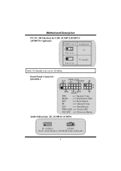
... ==> Power LED ON/ OFF ==> Power-on 5V Standby Note: 5V Standby only use for USB: JUSBV1/JUSBV2/ (JUSBV4=>optional) JUSBV1/ 2/ 4 Assignment 1 5V Pin 1-2 on 1 Pin 2-3 on Button Audio Subsystem: JF_AUDIO1/ JCDIN1 2 1 1 JFJA_AUUDDIOIO11 JCDIN1 (Front Audio Header) (CD-ROM Audio-In Header) 8 MMootthheerrbbooaarrdd DDeessccrriippttiioonn 5V/ 5V_SB Selection for S3 Mode. Front Panel Connector: JPANEL1 PWR_LED SLP ON/OFF IR 2 24 1 23 SPK (H+)L(E-)DRST IR SPK HLED RST IR ==> Speaker Conn. ==> Hard Driver LED ==> Reset Button...
... ==> Power LED ON/ OFF ==> Power-on 5V Standby Note: 5V Standby only use for USB: JUSBV1/JUSBV2/ (JUSBV4=>optional) JUSBV1/ 2/ 4 Assignment 1 5V Pin 1-2 on 1 Pin 2-3 on Button Audio Subsystem: JF_AUDIO1/ JCDIN1 2 1 1 JFJA_AUUDDIOIO11 JCDIN1 (Front Audio Header) (CD-ROM Audio-In Header) 8 MMootthheerrbbooaarrdd DDeessccrriippttiioonn 5V/ 5V_SB Selection for S3 Mode. Front Panel Connector: JPANEL1 PWR_LED SLP ON/OFF IR 2 24 1 23 SPK (H+)L(E-)DRST IR SPK HLED RST IR ==> Speaker Conn. ==> Hard Driver LED ==> Reset Button...
M7NCG 400 user's manual
Page 11
... 3 Mic Power 4 Audio Power 5 RT Line Out 6 RT Line Out 7 Reserved 8 Key 9 LFT Line Out 10 LFT Line Out JF_AUDIO1 only support 2CH. Clear CMOS Jumper: JCMOS JCMOS Assignment Pin 1-2 on Normal Operation 1 (default) Pin 2-3 on Clear CMOS Data 1 9 Audio line out and mic in signals are routed to the back panel audio line out connector. Front Panel Audio Connector/ Jumper Block Jumper Setting 12 3 5 7 4 6 Pin 5 and 6 Pin 9 and 10 9 10 1 3 5 7 9 246 No jumpers 10 installed Configuration Audio line...
... 3 Mic Power 4 Audio Power 5 RT Line Out 6 RT Line Out 7 Reserved 8 Key 9 LFT Line Out 10 LFT Line Out JF_AUDIO1 only support 2CH. Clear CMOS Jumper: JCMOS JCMOS Assignment Pin 1-2 on Normal Operation 1 (default) Pin 2-3 on Clear CMOS Data 1 9 Audio line out and mic in signals are routed to the back panel audio line out connector. Front Panel Audio Connector/ Jumper Block Jumper Setting 12 3 5 7 4 6 Pin 5 and 6 Pin 9 and 10 9 10 1 3 5 7 9 246 No jumpers 10 installed Configuration Audio line...
M7NCG 400 user's manual
Page 12
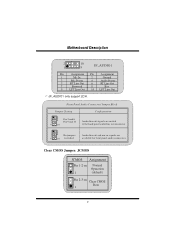
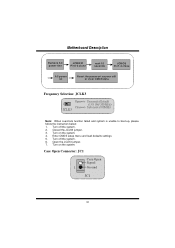
Open the JCLK3 jumper. 7. Enter CMOS setup menu and load defaults settings. 5. Turn on the system. 4. Case Open Connector: JC1 Case Open Signal 1 Ground JC1 10 Turn off the system. 6. Turn on the system. Closed the JCLK3 jumper. 3. MMootthheerrbbooaarrdd DDeessccrriippttiioonn Remove AC power line JCMOS1 Pin2-3 close wait 15 seconds JCMOS Pin1-2 close AC power on Reset the passwort as your will or clear CMOS data Frequency Selection: JCLK3 Open==> User mode (Default) 1 ((D1e3f3a/u1lt6)6/ 200...
Open the JCLK3 jumper. 7. Enter CMOS setup menu and load defaults settings. 5. Turn on the system. 4. Case Open Connector: JC1 Case Open Signal 1 Ground JC1 10 Turn off the system. 6. Turn on the system. Closed the JCLK3 jumper. 3. MMootthheerrbbooaarrdd DDeessccrriippttiioonn Remove AC power line JCMOS1 Pin2-3 close wait 15 seconds JCMOS Pin1-2 close AC power on Reset the passwort as your will or clear CMOS data Frequency Selection: JCLK3 Open==> User mode (Default) 1 ((D1e3f3a/u1lt6)6/ 200...
M7NCG 400 user's manual
Page 13
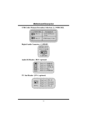
MMootthheerrbbooaarrdd DDeessccrriippttiioonn CNR Codec Primary/Secondary Selection: J_CODECSEL J_CODECSEL Pin 1-2 1 Pin 2-3 1 Assignment On-board Primary Codec. Digital Audio Connector: J_SPDIF1 SPDIF_OUT VCC5 GND 1 J_SPDIF1 Audio DJ Header: JDJ1 (optional) 1 5 JDJ1 Pin1 ==> SMBDT Pin2 ==> SMBCK Pin3 ==> -INTR_B Pin4 ==> Key Pin5 ==> PWRGD TV Out Header: JTV1 (optional) 24 13 JTV1 Pin1 ==> TV_Y Pin2 ==> Ground Pin3 ==> Ground Pin4 ==> TV_C 11 CNR Primary Codec.
MMootthheerrbbooaarrdd DDeessccrriippttiioonn CNR Codec Primary/Secondary Selection: J_CODECSEL J_CODECSEL Pin 1-2 1 Pin 2-3 1 Assignment On-board Primary Codec. Digital Audio Connector: J_SPDIF1 SPDIF_OUT VCC5 GND 1 J_SPDIF1 Audio DJ Header: JDJ1 (optional) 1 5 JDJ1 Pin1 ==> SMBDT Pin2 ==> SMBCK Pin3 ==> -INTR_B Pin4 ==> Key Pin5 ==> PWRGD TV Out Header: JTV1 (optional) 24 13 JTV1 Pin1 ==> TV_Y Pin2 ==> Ground Pin3 ==> Ground Pin4 ==> TV_C 11 CNR Primary Codec.

M7NCG 400 user's manual
Page 14
MMootthheerrbbooaarrdd DDeessccrriippttiioonn Back Panel Connectors JKBMS1 JUSBLAN1 PS/2 LAN(Optional) Mouse JPRNT1 Parallel JGAME1 Game Port PS/2 USB Keyboard COM1 JCOM1 Speaker Line In Mic COM2 Out In (optional) JCOM2 (optional) JKBMS1 JUSBLAN1 PS/2 LAN(Optional) Mouse JPRNT1 Parallel JGAME1 Game Port PS/2 USB Keyboard COM1 JCOM1 VGA1 JVGA1 Speaker Out Line In Mic In The LED indicator for Lan port status: Status Speed Normal 10Mbps Right light: green Left light: no 100Mbps Right light: green Left light: orange Download Light: blink Light: blink 12
MMootthheerrbbooaarrdd DDeessccrriippttiioonn Back Panel Connectors JKBMS1 JUSBLAN1 PS/2 LAN(Optional) Mouse JPRNT1 Parallel JGAME1 Game Port PS/2 USB Keyboard COM1 JCOM1 Speaker Line In Mic COM2 Out In (optional) JCOM2 (optional) JKBMS1 JUSBLAN1 PS/2 LAN(Optional) Mouse JPRNT1 Parallel JGAME1 Game Port PS/2 USB Keyboard COM1 JCOM1 VGA1 JVGA1 Speaker Out Line In Mic In The LED indicator for Lan port status: Status Speed Normal 10Mbps Right light: green Left light: no 100Mbps Right light: green Left light: orange Download Light: blink Light: blink 12
M7NCG 400 user's manual
Page 29
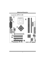
MMootthheerrbbooaarrdd DDeessccrriippttiioonn Layout des M7NCG 400 JKBMS1 JKBV1 1 JUSBLAN1 JCOM1 1 JUSBV2 JPRNT1 1 JCFAN1 FDD1 JATXPWER1 FLOPPY DISK CONN. DIMMB1 DIMMB2 DIMMA1 1 JCLK3 JTV1 24 13 JVGA1 JSPKR1 SP-OUT Winbond I/O GAME Port JLIN1 LINE-IN 5 JMIC1 MIC-IN 1 JGAME1 1 JDJ1 JNFAN1 Lan Chip 9 1 10 2 IGP PCI1 Codec 1 1 J_CODECSEL PCI2 PCI3 9 19 1 10 210 2 J1394A J1394B IDE2 IDE1 1394A Chip (optional) MCP...
MMootthheerrbbooaarrdd DDeessccrriippttiioonn Layout des M7NCG 400 JKBMS1 JKBV1 1 JUSBLAN1 JCOM1 1 JUSBV2 JPRNT1 1 JCFAN1 FDD1 JATXPWER1 FLOPPY DISK CONN. DIMMB1 DIMMB2 DIMMA1 1 JCLK3 JTV1 24 13 JVGA1 JSPKR1 SP-OUT Winbond I/O GAME Port JLIN1 LINE-IN 5 JMIC1 MIC-IN 1 JGAME1 1 JDJ1 JNFAN1 Lan Chip 9 1 10 2 IGP PCI1 Codec 1 1 J_CODECSEL PCI2 PCI3 9 19 1 10 210 2 J1394A J1394B IDE2 IDE1 1394A Chip (optional) MCP...
M7NCG 400 user's manual
Page 42
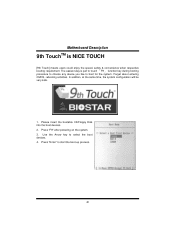
... very safe. 1. Please insert the bootable CD/Floppy Disk into the boot devices. 2. Use the Arrow key to start the boot-up process. 40 MMootthheerrbbooaarrdd DDeessccrriippttiioonn 9th TouchTM is just to touch 「F9」 function key during booting procedure to choose any device you like to boot for the system. Press "Enter" to select the boot devices. 4. Forget about entering CMOS, rebooting activities. Press "F9" after powering on...
... very safe. 1. Please insert the bootable CD/Floppy Disk into the boot devices. 2. Use the Arrow key to start the boot-up process. 40 MMootthheerrbbooaarrdd DDeessccrriippttiioonn 9th TouchTM is just to touch 「F9」 function key during booting procedure to choose any device you like to boot for the system. Press "Enter" to select the boot devices. 4. Forget about entering CMOS, rebooting activities. Press "F9" after powering on...
M7NCG 400 user's manual
Page 43
BIOSTAR's [FLASHER™] technology integrates flash utility function onto BIOS firmware. Download the latest BIOS file from the BIOSTAR website to enter CMOS setup. 5. Insert the disk that contains the newest BIOS file into the floppy drive. 3. Power ON the computer. 4. Press [DEL] to a floppy disk. 2. Flasher Step by Step 1. Unfortunately, there is users do it takes time to prepare the utility. MMootthheerrbbooaarrdd DDeessccrriippttiioonn BIOS STAR -[ FLASHER™ ] Regularly, when users want to update BIOS, there are two...
BIOSTAR's [FLASHER™] technology integrates flash utility function onto BIOS firmware. Download the latest BIOS file from the BIOSTAR website to enter CMOS setup. 5. Insert the disk that contains the newest BIOS file into the floppy drive. 3. Power ON the computer. 4. Press [DEL] to a floppy disk. 2. Flasher Step by Step 1. Unfortunately, there is users do it takes time to prepare the utility. MMootthheerrbbooaarrdd DDeessccrriippttiioonn BIOS STAR -[ FLASHER™ ] Regularly, when users want to update BIOS, there are two...
M7NCG 400 user's manual
Page 44
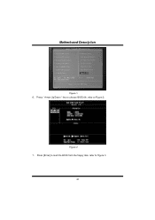
MMootthheerrbbooaarrdd DDeessccrriippttiioonn Figure 1 6. Press " Arrow Up/Down " key to choose BIOS file, refer to Figure 3. 42 Press [Enter] to load the BIOS from the floppy disk, refer to Figure 2 Figure 2 7.
MMootthheerrbbooaarrdd DDeessccrriippttiioonn Figure 1 6. Press " Arrow Up/Down " key to choose BIOS file, refer to Figure 3. 42 Press [Enter] to load the BIOS from the floppy disk, refer to Figure 2 Figure 2 7.
M7NCG 400 user's manual
Page 46
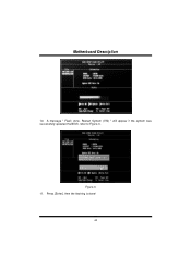
Figure 6 11. MMootthheerrbbooaarrdd DDeessccrriippttiioonn 10. A message " Flash done, Restart System (Y/N) " will appear if the system was successfully updated the BIOS, refer to Figure 6. Press [Enter], then the flashing is done! 44
Figure 6 11. MMootthheerrbbooaarrdd DDeessccrriippttiioonn 10. A message " Flash done, Restart System (Y/N) " will appear if the system was successfully updated the BIOS, refer to Figure 6. Press [Enter], then the flashing is done! 44
M7NCG 400 user's manual
Page 47
... over -clocking that when overclocking, the system can save you from rebooting in the BIOS setting. This user-friendly design can be at a safe and sound! 45 After that, press and power on opening the case just to clear the CMOS. In the end, thanks to the Watchdog Technology, everything is important to know that reaches the threshold settings, the Watchdog Technology will disable your...
... over -clocking that when overclocking, the system can save you from rebooting in the BIOS setting. This user-friendly design can be at a safe and sound! 45 After that, press and power on opening the case just to clear the CMOS. In the end, thanks to the Watchdog Technology, everything is important to know that reaches the threshold settings, the Watchdog Technology will disable your...
M7NCG 400 user's manual
Page 48
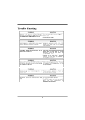
... be used but booting the hard drive. Make sure "CMOS Failure." Call drive manufacturers for compatibility with other drives. 46 Indicator light on keyboard does not turn * Replace cable * Contact technical support PROBABLE SOLUTION System inoperative. PROBABLE SOLUTION Screen message says "Invalid Configuration" or * Review system's equipment . correct information is extremely important. Keyboard lights are on, power * Using even pressure on both ends are securely plugged in illuminate, fan inside power supply does not on turn on...
... be used but booting the hard drive. Make sure "CMOS Failure." Call drive manufacturers for compatibility with other drives. 46 Indicator light on keyboard does not turn * Replace cable * Contact technical support PROBABLE SOLUTION System inoperative. PROBABLE SOLUTION Screen message says "Invalid Configuration" or * Review system's equipment . correct information is extremely important. Keyboard lights are on, power * Using even pressure on both ends are securely plugged in illuminate, fan inside power supply does not on turn on...


