Service Manual
Page 4
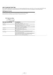
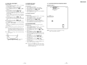
... standards. /Replace the disc, and repeat the recording procedure. Should any problem persist, consult your nearest Sony dealer. Self-diagnosis display C11 Protected Three-digit display/Message C11/Protected C13/REC Error C13/Disc Error C14/Disc Error C71/Din Unlock Cause/Remedy The inserted MD is dirty (with smudges, fingerprints, etc.) scratched...
... standards. /Replace the disc, and repeat the recording procedure. Should any problem persist, consult your nearest Sony dealer. Self-diagnosis display C11 Protected Three-digit display/Message C11/Protected C13/REC Error C13/Disc Error C14/Disc Error C71/Din Unlock Cause/Remedy The inserted MD is dirty (with smudges, fingerprints, etc.) scratched...
Service Manual
Page 16
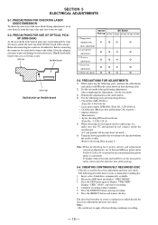
... 5) When observing several signals on page 4.) Note :When performing laser power checks and adjustment (electrical adjustment), use of the new MD laser power meter 8010S (J-2501-145-A) instead of the conventional laser power meter is convenient. Before disconnecting the connector, desolder first. ...rate check. Traverse ¬ ¬ G ¬ adjustment 4. Focus bias ¬ ¬ G ¬ adjustment 5. CREATING CONTINUOUSLY RECORDED DISC • This disc is easily damaged by static electricity. Press the §EJECT button and remove the disc. Press the YES button...
... 5) When observing several signals on page 4.) Note :When performing laser power checks and adjustment (electrical adjustment), use of the new MD laser power meter 8010S (J-2501-145-A) instead of the conventional laser power meter is convenient. Before disconnecting the connector, desolder first. ...rate check. Traverse ¬ ¬ G ¬ adjustment 4. Focus bias ¬ ¬ G ¬ adjustment 5. CREATING CONTINUOUSLY RECORDED DISC • This disc is easily damaged by static electricity. Press the §EJECT button and remove the disc. Press the YES button...
Service Manual
Page 18
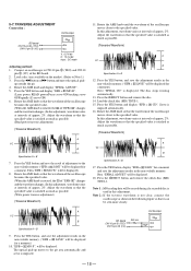
... AMS knob so that the specified value is imposed. The disc stops rotating automatically. 13. Press the §EJECT button and remove the check disc (MD) TDYS-1. A VC B Specification A = B 9. Rotate the AMS knob so that the specified value is imposed automatically. 16. Adjust the waveform so ... value. Rotate the AMS knob until the waveform of the BD board. 2. Adjust the waveform so that it can be erased during if a recorded disc is satisfied as much as shown in this adjustment, waveform varies at intervals of approx. 2%. Note 2 : If the traverse waveform is ...
... AMS knob so that the specified value is imposed. The disc stops rotating automatically. 13. Press the §EJECT button and remove the check disc (MD) TDYS-1. A VC B Specification A = B 9. Rotate the AMS knob so that the specified value is imposed automatically. 16. Adjust the waveform so ... value. Rotate the AMS knob until the waveform of the BD board. 2. Adjust the waveform so that it can be erased during if a recorded disc is satisfied as much as shown in this adjustment, waveform varies at intervals of approx. 2%. Note 2 : If the traverse waveform is ...
Service Manual
Page 19
... knob and display "FBIAS CHECK". 6. Press the EDIT/NO button, next press the §EJECT button, and remove the continuously recorded disc. Load a check disc (MD) TDYS-1. 2. Press the YES button twice and display "CPLAY MID". 4. Rotate the AMS knob and display "FBIAS ADJUST". 6...., check that the C1 error rate is automatically calculated from step 2. 13. 5-8. Press the YES button and display " / a = ". Load a continuously recorded disc (Refer to "5-4. Note 1 : If the C1 error and ADER are above adjustment. Press the EDIT/NO button when "C1 = AD = " is...
... knob and display "FBIAS CHECK". 6. Press the EDIT/NO button, next press the §EJECT button, and remove the continuously recorded disc. Load a check disc (MD) TDYS-1. 2. Press the YES button twice and display "CPLAY MID". 4. Rotate the AMS knob and display "FBIAS ADJUST". 6...., check that the C1 error rate is automatically calculated from step 2. 13. 5-8. Press the YES button and display " / a = ". Load a continuously recorded disc (Refer to "5-4. Note 1 : If the C1 error and ADER are above adjustment. Press the EDIT/NO button when "C1 = AD = " is...
Service Manual
Page 20
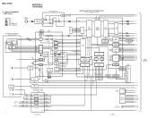
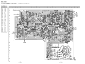
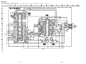
... LDON WRPWR MOD SDA SCL LIMIT REFLECT PROTECT CHUCK IN PACK OUT PB P REC P M903 LOADING MOTOR M LOAD-IN LOAD-OUT XRST - 22 - M SPDL+ SPDL- MDS-JE320 6-1. APC APCREF EQADJ 3TADJ WBLADJ SPRD SPFD FG IN XRST RECP APCREF FFDR FRDR TFDR TRDR SFDR SRDR MORFO MORFI RFO AGCI FILTER TX...
... LDON WRPWR MOD SDA SCL LIMIT REFLECT PROTECT CHUCK IN PACK OUT PB P REC P M903 LOADING MOTOR M LOAD-IN LOAD-OUT XRST - 22 - M SPDL+ SPDL- MDS-JE320 6-1. APC APCREF EQADJ 3TADJ WBLADJ SPRD SPFD FG IN XRST RECP APCREF FFDR FRDR TFDR TRDR SFDR SRDR MORFO MORFI RFO AGCI FILTER TX...
Service Manual
Page 21
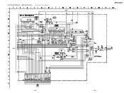
..., 310 RECT D303, 304 RECT D301, 302 RECT D305, 306 AC FL701 AC TR301 POWER TRANSFORMER L IN R J301 LINE (ANALOG) R OUT L AC IN - 23 - - 24 - MDS-JE320 - DIN IC314 12 13 DIGITAL OPTICAL IN 3 IC353 ADDT DADT SCTX XINT BCK LRCK 512FS SQSY DQSY MNT3 MNT2 MNT1 MNT0 SENS SRDT SCLK...
..., 310 RECT D303, 304 RECT D301, 302 RECT D305, 306 AC FL701 AC TR301 POWER TRANSFORMER L IN R J301 LINE (ANALOG) R OUT L AC IN - 23 - - 24 - MDS-JE320 - DIN IC314 12 13 DIGITAL OPTICAL IN 3 IC353 ADDT DADT SCTX XINT BCK LRCK 512FS SQSY DQSY MNT3 MNT2 MNT1 MNT0 SENS SRDT SCLK...
Service Manual
Page 22
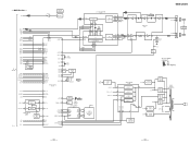
...-T) 0.1Vp-p 32.77kHz 2.6Vp-p 3 IC101 8,9 E, F (PLAY mode) 3 IC307 0 (LRCK1), @• (LRCK2) • U : B+ Line. • V : B- Voltage variations may be noted due to waveforms. • Signal path. MDS-JE320 6-2. CIRCUIT BOARDS LOCATION SW board DISPLAY board BD board EJECT SW board CONTROL (SW) board - 25 - E :PB q :REC r :REC(DIGITAL IN) a :REC(DIGITAL OUT...
...-T) 0.1Vp-p 32.77kHz 2.6Vp-p 3 IC101 8,9 E, F (PLAY mode) 3 IC307 0 (LRCK1), @• (LRCK2) • U : B+ Line. • V : B- Voltage variations may be noted due to waveforms. • Signal path. MDS-JE320 6-2. CIRCUIT BOARDS LOCATION SW board DISPLAY board BD board EJECT SW board CONTROL (SW) board - 25 - E :PB q :REC r :REC(DIGITAL IN) a :REC(DIGITAL OUT...
Service Manual
Page 23
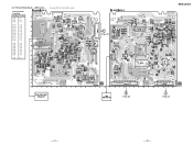
BD Section - • See page 25 for Circuit Boards Location. • Semiconductor Location Ref. Printed Wiring Board - No. Location D101 E-3 D181 C-9 D183 C-9 IC101 F-14 IC103 B-15 IC121 D-12 IC122 C-4 IC123 E-10 IC124 F-12 IC152 B-12 IC171 F-9 IC181 D-9 IC192 G-6 Q101 C-14 Q102 B-15 Q103 B-14 Q104 B-14 Q162 B-14 Q163 B-15 Q180 D-6 Q181 B-9 Q182 B-9 (Page 45) 16 (Page 33) MDS-JE320 (Page 33) - 27 - - 28 - 6-3.
BD Section - • See page 25 for Circuit Boards Location. • Semiconductor Location Ref. Printed Wiring Board - No. Location D101 E-3 D181 C-9 D183 C-9 IC101 F-14 IC103 B-15 IC121 D-12 IC122 C-4 IC123 E-10 IC124 F-12 IC152 B-12 IC171 F-9 IC181 D-9 IC192 G-6 Q101 C-14 Q102 B-15 Q103 B-14 Q104 B-14 Q162 B-14 Q163 B-15 Q180 D-6 Q181 B-9 Q182 B-9 (Page 45) 16 (Page 33) MDS-JE320 (Page 33) - 27 - - 28 - 6-3.
Service Manual
Page 24
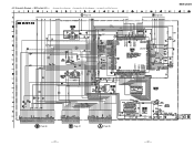
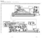
Schematic Diagram - MDS-JE320 6-4. BD Section (1/2)- • See page 26 for Waveforms. • See page 49 for IC Block Diagrams. • See page 54 for IC Pin Functions. 16 (Page 31) - 29 - (Page 32) - 30 -
Schematic Diagram - MDS-JE320 6-4. BD Section (1/2)- • See page 26 for Waveforms. • See page 49 for IC Block Diagrams. • See page 54 for IC Pin Functions. 16 (Page 31) - 29 - (Page 32) - 30 -
Service Manual
Page 25
BD Section (2/2) - • See page 26 for Waveforms. • See page 49 for IC Block Diagrams. • See page 54 for IC Pin Functions. (Page 29) (Page 30) MDS-JE320 BR24C01AF 16 (Page 36) (Page 47) (Page 35) - 31 - - 32 - 6-5. Schematic Diagram -
BD Section (2/2) - • See page 26 for Waveforms. • See page 49 for IC Block Diagrams. • See page 54 for IC Pin Functions. (Page 29) (Page 30) MDS-JE320 BR24C01AF 16 (Page 36) (Page 47) (Page 35) - 31 - - 32 - 6-5. Schematic Diagram -
Service Manual
Page 26
... - 1 5 X X NOT REPLACEABLE: BUILT IN TRANSFORMER - 34 - 1-665-005- 21 AC IN Main Section - • See page 25 for Circuit Boards Location. • Semiconductor Location Ref. MDS-JE320 6-6.
... - 1 5 X X NOT REPLACEABLE: BUILT IN TRANSFORMER - 34 - 1-665-005- 21 AC IN Main Section - • See page 25 for Circuit Boards Location. • Semiconductor Location Ref. MDS-JE320 6-6.

Service Manual
Page 27
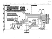
Main Section (1/3) - • See page 26 for Waveforms • See page 54 for IC Pin Functions. 6-7. MDS-JE320 (PAGE 32) - 35 - (PAGE 31) - 36 - Schematic Diagram -
Main Section (1/3) - • See page 26 for Waveforms • See page 54 for IC Pin Functions. 6-7. MDS-JE320 (PAGE 32) - 35 - (PAGE 31) - 36 - Schematic Diagram -
Service Manual
Page 28
MDS-JE320 6-8. Main Section (2/3) - • See page 26 for Waveforms. • See page 49 for IC Block Diagrams. • See page 54 for IC Pin Functions. - 37 - - 38 - Schematic Diagram -
MDS-JE320 6-8. Main Section (2/3) - • See page 26 for Waveforms. • See page 49 for IC Block Diagrams. • See page 54 for IC Pin Functions. - 37 - - 38 - Schematic Diagram -
Service Manual
Page 29
MDS-JE320 (PAGE 44) - 39 - - 40 - 6-9. Main Section (3/3) - • See page 49 for IC Block Diagram. Schematic Diagram -
MDS-JE320 (PAGE 44) - 39 - - 40 - 6-9. Main Section (3/3) - • See page 49 for IC Block Diagram. Schematic Diagram -
Service Manual
Page 30
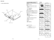
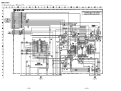
Printed Wiring Board - DISPLAY Section - • See page 25 for Circuit Boards Location. 1 2 3 4 5 6 7 8 9 A DISPLAY BOARD B C FLUORESCENT INDICATOR TUBE D 10 11 12 E E S764 1 3 21 1-661-891- (21) E F CONTROL (SW) BOARD REC LEVEL G H INPUT DIGITAL ANALOG C (PAGE 33) S762 DISPLAY/CHAR S774 S775 AMS (PUSH ENTER) 5 4 1 3 EJECT SW BOARD 1 S776 EJECT 3 CN705 21 1-661-893- (21) 1 3 I S771 S772 S780 S781 S752 S751 REC YES NO/EDIT 16 21 1-661-890- (21) - 41 - - 42 - MDS-JE320 6-10.
Printed Wiring Board - DISPLAY Section - • See page 25 for Circuit Boards Location. 1 2 3 4 5 6 7 8 9 A DISPLAY BOARD B C FLUORESCENT INDICATOR TUBE D 10 11 12 E E S764 1 3 21 1-661-891- (21) E F CONTROL (SW) BOARD REC LEVEL G H INPUT DIGITAL ANALOG C (PAGE 33) S762 DISPLAY/CHAR S774 S775 AMS (PUSH ENTER) 5 4 1 3 EJECT SW BOARD 1 S776 EJECT 3 CN705 21 1-661-893- (21) 1 3 I S771 S772 S780 S781 S752 S751 REC YES NO/EDIT 16 21 1-661-890- (21) - 41 - - 42 - MDS-JE320 6-10.
Service Manual
Page 31
DISPLAY Section - • See page 26 for Waveforms. - 43 - Schematic Diagram - MDS-JE320 (PAGE 39) - 44 - 6-11.
DISPLAY Section - • See page 26 for Waveforms. - 43 - Schematic Diagram - MDS-JE320 (PAGE 39) - 44 - 6-11.
Service Manual
Page 32
Printed Wiring Board - Switch Section - • See page 25 for Circuit Boards Location. 1 2 3 4 5 6 7 8 9 10 11 12 13 A B C (Page 28) D E F G H I J 16 - 45 - - 46 - MDS-JE320 6-12.
Printed Wiring Board - Switch Section - • See page 25 for Circuit Boards Location. 1 2 3 4 5 6 7 8 9 10 11 12 13 A B C (Page 28) D E F G H I J 16 - 45 - - 46 - MDS-JE320 6-12.
Service Manual
Page 56
... R378 R383 Part No. Ne les remplacer que par une pièce portant le numéro spécifié. 9-922-894-11 Sony Corporation Home A&V Products Company - 72 - 98F1664-1 Printed in Japan ©1998.6 Published by mark ! No. No. are critical for safety. Description 1-249-441-11 1-249... PIC-UP KMS-260A/J1NP 1-500-396-11 HEAD, OVER WRITE A-4672-135-A MOTOR ASSY, SPINDLE M902 M903 ! TR301 ! Replace only with mark ! Part No. MDS-JE320 MAIN SW Ref.
... R378 R383 Part No. Ne les remplacer que par une pièce portant le numéro spécifié. 9-922-894-11 Sony Corporation Home A&V Products Company - 72 - 98F1664-1 Printed in Japan ©1998.6 Published by mark ! No. No. are critical for safety. Description 1-249-441-11 1-249... PIC-UP KMS-260A/J1NP 1-500-396-11 HEAD, OVER WRITE A-4672-135-A MOTOR ASSY, SPINDLE M902 M903 ! TR301 ! Replace only with mark ! Part No. MDS-JE320 MAIN SW Ref.