Service Manual
Page 1
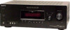
... of Dolby Laboratories. HDMI, the HDMI logo and High-Definition Multimedia Interface are trademarks of HDMI Licensing LLC. MULTI CHANNEL AV RECEIVER 9-887-608-01 2007C04-1 © 2007.03 Sony Corporation Home Audio Division Published by Sony Techno Create Corporation 1 This receiver incorporates High-Definition Multimedia... total harmonic distortion from 120 - 20,000 Hz; Depending on next page - SERVICE MANUAL Ver. 1.0 2007.03 STR-K7100 US Model Manufactured under the following conditions: Area code US Power requirements 120 V AC, 60 Hz 2) Reference power...
... of Dolby Laboratories. HDMI, the HDMI logo and High-Definition Multimedia Interface are trademarks of HDMI Licensing LLC. MULTI CHANNEL AV RECEIVER 9-887-608-01 2007C04-1 © 2007.03 Sony Corporation Home Audio Division Published by Sony Techno Create Corporation 1 This receiver incorporates High-Definition Multimedia... total harmonic distortion from 120 - 20,000 Hz; Depending on next page - SERVICE MANUAL Ver. 1.0 2007.03 STR-K7100 US Model Manufactured under the following conditions: Area code US Power requirements 120 V AC, 60 Hz 2) Reference power...
Service Manual
Page 4
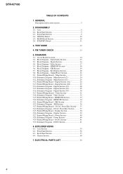
... Power Key Section - ........ 37 5-25. Schematic Diagram - Front Panel Section 56 6-3. Chassis Section 58 7. Tuner/Audio Section 15 5-3. Video Section 17 5-5. Key/Display Section 20 5-8. Main Section 23 5-10. Printed Wiring Board - ...HDMI SW Section 18 5-6. Printed Wiring Board - Display Section 38 5-26. Printed Wiring Board - Case 8 2-2. Block Diagram - Digital Section (2/2 27 5-14. Printed Wiring Boards - Schematic Diagram - Printed Wiring Boards - Main Section (1/2 24 5-11. Printed Wiring Board - EXPLODED VIEWS 6-1. STR-K7100...
... Power Key Section - ........ 37 5-25. Schematic Diagram - Front Panel Section 56 6-3. Chassis Section 58 7. Tuner/Audio Section 15 5-3. Video Section 17 5-5. Key/Display Section 20 5-8. Main Section 23 5-10. Printed Wiring Board - ...HDMI SW Section 18 5-6. Printed Wiring Board - Display Section 38 5-26. Printed Wiring Board - Case 8 2-2. Block Diagram - Digital Section (2/2 27 5-14. Printed Wiring Boards - Schematic Diagram - Printed Wiring Boards - Main Section (1/2 24 5-11. Printed Wiring Board - EXPLODED VIEWS 6-1. STR-K7100...
Service Manual
Page 6
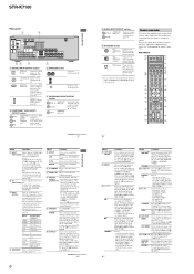
...Name Function ./>b) Press to start playback of all components, press ?/1 and AV ?/1 (A) at the same time, it will turn off . PRESET +a)/- ...m/Mb) Function Press to control non-Sony audio/video components. MUTING Press to select A.F.D. Note The function of the input buttons, the receiver turns on the TV screen. Press ...HDMI OUT or MONITOR OUT jack to control non-Sony components following the steps in recording standby.) Press to stop playback of the buttons to select the TV channels. Press 0/10 to a DVD IN jack player, etc. Q TV VOL +/- STR-K7100...
...Name Function ./>b) Press to start playback of all components, press ?/1 and AV ?/1 (A) at the same time, it will turn off . PRESET +a)/- ...m/Mb) Function Press to control non-Sony audio/video components. MUTING Press to select A.F.D. Note The function of the input buttons, the receiver turns on the TV screen. Press ...HDMI OUT or MONITOR OUT jack to control non-Sony components following the steps in recording standby.) Press to stop playback of the buttons to select the TV channels. Press 0/10 to a DVD IN jack player, etc. Q TV VOL +/- STR-K7100...
Service Manual
Page 31
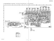
... IN VIDEO 1 IN -4 -7 -5 -8 -6 -9 J302 MONITOR OUT -1 Y -2 PB/CB -3 PR/CR C D E VIDEO 3 BOARD J298 VIDEO 3 IN/PORTABLE AV IN R299 BLK C293 C294 F CN202 -1 VIDEO C299 -2 -3 L AUDIO R G (CHASSIS) H R298 C298 C312 R309 HDMI SW P BOARD CN5004 (Page 33) CN204 GRY 7 GRY GRY GRY GRY RED 1 DIGITAL L BOARD CNS510 (Page 27) C207 JW205... C315 TP201 CL090 12 1-872-437- (12) R312 C316 • Semiconductor Location Ref. No. Location D203 D-8 D204 D-8 IC203 IC304 IC804 IC807 D-9 E-12 F-9 F-11 STR-K7100 31 31 STR-K7100 5-17. PRINTED WIRING BOARDS -
... IN VIDEO 1 IN -4 -7 -5 -8 -6 -9 J302 MONITOR OUT -1 Y -2 PB/CB -3 PR/CR C D E VIDEO 3 BOARD J298 VIDEO 3 IN/PORTABLE AV IN R299 BLK C293 C294 F CN202 -1 VIDEO C299 -2 -3 L AUDIO R G (CHASSIS) H R298 C298 C312 R309 HDMI SW P BOARD CN5004 (Page 33) CN204 GRY 7 GRY GRY GRY GRY RED 1 DIGITAL L BOARD CNS510 (Page 27) C207 JW205... C315 TP201 CL090 12 1-872-437- (12) R312 C316 • Semiconductor Location Ref. No. Location D203 D-8 D204 D-8 IC203 IC304 IC804 IC807 D-9 E-12 F-9 F-11 STR-K7100 31 31 STR-K7100 5-17. PRINTED WIRING BOARDS -
Service Manual
Page 32
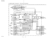
...STR-K7100 STR-K7100 1 3 4 5 6 7 1 2 3 4 5 6 7 8 9 10 11 12 13 G V1 V2 1 V3 2 3 G 4 V1 V2 G 5-18. SCHEMATIC DIAGRAM - VIDEO SECTION - • Refer to page 44 for IC Block Diagrams. 1 2 3 4 5 6 VIDEO 3 BOARD J298 A 3P -1 V VIDEO CN201 5P 1 R-CH (Page 24) MAIN VIDEO 3 IN/ PORTABLE AV IN -2 L L C299 R299 2 GND 3 L-CH F BOARD (1/2) CNP503 220p 1k 4 GND AUDIO...CL087 NC -15V MAIN E BOARD (1/2) CN505 (Page 24) CNS207 13P V MUTE HDMI 6.8V S2 {HDMI} S1 (HDMI} OEB {HDMI} PRE {HDMI} CTL {HDMI} COMP_S2 COMP_S1 V_SW1 V_SW2 V_SW3 V_SW4 CL088 CN204 6P CTL PRE OEB GND S1 +VC...
...STR-K7100 STR-K7100 1 3 4 5 6 7 1 2 3 4 5 6 7 8 9 10 11 12 13 G V1 V2 1 V3 2 3 G 4 V1 V2 G 5-18. SCHEMATIC DIAGRAM - VIDEO SECTION - • Refer to page 44 for IC Block Diagrams. 1 2 3 4 5 6 VIDEO 3 BOARD J298 A 3P -1 V VIDEO CN201 5P 1 R-CH (Page 24) MAIN VIDEO 3 IN/ PORTABLE AV IN -2 L L C299 R299 2 GND 3 L-CH F BOARD (1/2) CNP503 220p 1k 4 GND AUDIO...CL087 NC -15V MAIN E BOARD (1/2) CN505 (Page 24) CNS207 13P V MUTE HDMI 6.8V S2 {HDMI} S1 (HDMI} OEB {HDMI} PRE {HDMI} CTL {HDMI} COMP_S2 COMP_S1 V_SW1 V_SW2 V_SW3 V_SW4 CL088 CN204 6P CTL PRE OEB GND S1 +VC...
Service Manual
Page 50
STR-K7100 IC1907 MB91353APMT-G-112E1 (SYSTEM CONTROL) (DIGITAL BOARD (2/3)) Pin No. Ground pin 41 TC74HC153A O Input select switch control signal output A 42 TC74HC153B O Input select switch control signal output B 43 VSS - Pin Name I/O Pin Description 1 HDMI MUTE I HDMI mute signal input Not used in this set. (Open) 2 HDMI RESET/HDMI PRE O HDMI reset signal output 3 XM RESET O XM...
STR-K7100 IC1907 MB91353APMT-G-112E1 (SYSTEM CONTROL) (DIGITAL BOARD (2/3)) Pin No. Ground pin 41 TC74HC153A O Input select switch control signal output A 42 TC74HC153B O Input select switch control signal output B 43 VSS - Pin Name I/O Pin Description 1 HDMI MUTE I HDMI mute signal input Not used in this set. (Open) 2 HDMI RESET/HDMI PRE O HDMI reset signal output 3 XM RESET O XM...
Service Manual
Page 51
... IN I 88 HDMI CEC IN/HDMI OED I 89 HDMI UART IN/HDMI S1 I 90 HDMI UART OUT/HDMI S2 O 91 HDMI CEC OUT O 92 XM MIXMO I 93 XM MOXMI O 94 HDMI REG CTRL O 95 VCC I 96 VSS - 97 EEPROM DATA I/O 98 EEPROM CLK O 99 HD OUT I Pin Description Digital audio interface receiver error signal input Digital audio interface receiver state signal input...
... IN I 88 HDMI CEC IN/HDMI OED I 89 HDMI UART IN/HDMI S1 I 90 HDMI UART OUT/HDMI S2 O 91 HDMI CEC OUT O 92 XM MIXMO I 93 XM MOXMI O 94 HDMI REG CTRL O 95 VCC I 96 VSS - 97 EEPROM DATA I/O 98 EEPROM CLK O 99 HD OUT I Pin Description Digital audio interface receiver error signal input Digital audio interface receiver state signal input...


