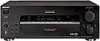
Service Manual
Page 2
... FM antenna adapter (1) STR-DB930, V929X only • Remote commander RM-LJ302 (remote) (1) • LR6 (size-AA) alkaline batteries (3) STR-DB830 only • Remote commander RM-PP402 (remote) (1) • LR6 (size-AA) batteries (2) Design and specifications are subject to change the tuning scale. To reset the... :290 W STR-DB830 North American models : 280 W AC outlets North American models : 2 switched, total 120 W/1A Other models : 1 switched, max 100 W Dimensions 430 × 405 × 160.5 mm (17 × 16 × 63/8 in any AM station, turn off the receiver. 5.1CH INPUT...
... FM antenna adapter (1) STR-DB930, V929X only • Remote commander RM-LJ302 (remote) (1) • LR6 (size-AA) alkaline batteries (3) STR-DB830 only • Remote commander RM-PP402 (remote) (1) • LR6 (size-AA) batteries (2) Design and specifications are subject to change the tuning scale. To reset the... :290 W STR-DB830 North American models : 280 W AC outlets North American models : 2 switched, total 120 W/1A Other models : 1 switched, max 100 W Dimensions 430 × 405 × 160.5 mm (17 × 16 × 63/8 in any AM station, turn off the receiver. 5.1CH INPUT...
Service Manual
Page 5
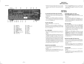
... on press the ENTER button. * Either the 9 kHz step or 10 kHz step can be caused by the DSP, the data output must not be received by tuner. AUTOBETICAL MODE (AEP Model only) * This mode is returned. SECTION 3 TEST MODE !¢ !£ !™ 9 FLUORESCENT INDICATOR TUBE ...the remote control. 2. When the front panel is removed, the VR board is connected. The message Factry Set appears and the present contents are reset to the default setting. * Procedure: While depressing the SET UP, the LEVEL and the ENTER buttons simultaneously, press the power [1/u] button to...
... on press the ENTER button. * Either the 9 kHz step or 10 kHz step can be caused by the DSP, the data output must not be received by tuner. AUTOBETICAL MODE (AEP Model only) * This mode is returned. SECTION 3 TEST MODE !¢ !£ !™ 9 FLUORESCENT INDICATOR TUBE ...the remote control. 2. When the front panel is removed, the VR board is connected. The message Factry Set appears and the present contents are reset to the default setting. * Procedure: While depressing the SET UP, the LEVEL and the ENTER buttons simultaneously, press the power [1/u] button to...
Service Manual
Page 6
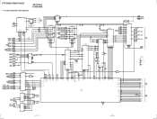
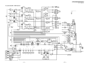
... L INPUT L SELECTOR IC303 27 23 26 25 24 20 22 21 17 CONTROL CE CLK DI 15 14 16 S LAT S CLK S DATA DIGITAL AUDIO I/F RECEIVER IC1101 DATA 16 CK OUT 13 3 D IN BCK 14 LRCK 15 12.288M 22 IC11404 IC1404 IC1404 36 DI 38 CLK 37 CE ERROR 34... SP RY U DATA U CLOCK U MREQ U SREQ U REST RESET RY POWER D STOP SOT0 SIN1 MD2 MD0 - 7 - - 8 - STR-DB830/DB930/V929X 4-1. BLOCK DIAGRAM MAIN SECTION SECTION 4 DIAGRAMS TM301 ANTENNA FM 75Ω AM TUNER UNIT FM AM ANT LEVEL 6 FM DET 9 L OUT 10 RDS 2 4 IC1 16 13 14 X1 4.33MHz AEP ONLY R OUT 12 R CH DO TUNED STEREO T.
... L INPUT L SELECTOR IC303 27 23 26 25 24 20 22 21 17 CONTROL CE CLK DI 15 14 16 S LAT S CLK S DATA DIGITAL AUDIO I/F RECEIVER IC1101 DATA 16 CK OUT 13 3 D IN BCK 14 LRCK 15 12.288M 22 IC11404 IC1404 IC1404 36 DI 38 CLK 37 CE ERROR 34... SP RY U DATA U CLOCK U MREQ U SREQ U REST RESET RY POWER D STOP SOT0 SIN1 MD2 MD0 - 7 - - 8 - STR-DB830/DB930/V929X 4-1. BLOCK DIAGRAM MAIN SECTION SECTION 4 DIAGRAMS TM301 ANTENNA FM 75Ω AM TUNER UNIT FM AM ANT LEVEL 6 FM DET 9 L OUT 10 RDS 2 4 IC1 16 13 14 X1 4.33MHz AEP ONLY R OUT 12 R CH DO TUNED STEREO T.
Service Manual
Page 7
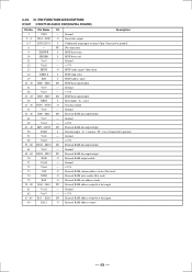
...F901 EXCEPT US,Canadian MODEL F903 US,Canadian MODEL JW925 CNJ901 CNP901 AC IN STR-DB830/DB930/V929X Ver 1.1 2002. 02 4-2. BLOCK DIAGRAM POWER SECTION L C...J701 PHONES L A TM501 R FRONT SPEAKER L B R • R-CH is omitted due to same as L-CH. • Signal Path :FM :CD C TM701 S(L) SURROUND SPEAKER S(R) L JJ101 SUB WOOFER R L REAR R L FRONT R JJ102 CENTER +5V PRE OUT +15V -15V ...5V DIGITAL +5V CONT µCOM ETC DISP µCOM+5.6V D1208 IC101 REMOTO CONTROL RECEIVER RESET Q103 D1211 +6.2 REG Q1205 3 8 RESET 5 IC1206 6 IC1207 3 +5V REG 1 IC1501 3 +5V REG 1 IC1203 3...
...F901 EXCEPT US,Canadian MODEL F903 US,Canadian MODEL JW925 CNJ901 CNP901 AC IN STR-DB830/DB930/V929X Ver 1.1 2002. 02 4-2. BLOCK DIAGRAM POWER SECTION L C...J701 PHONES L A TM501 R FRONT SPEAKER L B R • R-CH is omitted due to same as L-CH. • Signal Path :FM :CD C TM701 S(L) SURROUND SPEAKER S(R) L JJ101 SUB WOOFER R L REAR R L FRONT R JJ102 CENTER +5V PRE OUT +15V -15V ...5V DIGITAL +5V CONT µCOM ETC DISP µCOM+5.6V D1208 IC101 REMOTO CONTROL RECEIVER RESET Q103 D1211 +6.2 REG Q1205 3 8 RESET 5 IC1206 6 IC1207 3 +5V REG 1 IC1501 3 +5V REG 1 IC1203 3...
Service Manual
Page 27
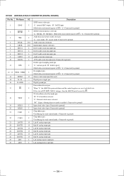
... data read Ground +3.3V HCIF ready signal Open drain HCIF chip select HCIF address input HCIF data input/output Ground +3.3V HCIF data input/output Reset input "L": active Test data output Ground External RAM data input/output Ground +3.3V External RAM data input/output Test data input "L" = normal "H" = test (Connected to...
... data read Ground +3.3V HCIF ready signal Open drain HCIF chip select HCIF address input HCIF data input/output Ground +3.3V HCIF data input/output Reset input "L": active Test data output Ground External RAM data input/output Ground +3.3V External RAM data input/output Test data input "L" = normal "H" = test (Connected to...
Service Manual
Page 29
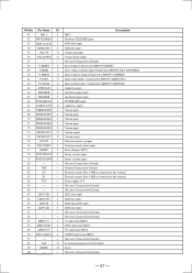
... I/O 23 HD1 O To CXD2712 HCIF data I/O 24 HD0 O To CXD2712 HCIF data I/O 25 HA0 O To CXD2712 address 26 XRST O To CXD2712 reset 27 HRDY I To CXD2712 ready 28 CS O To AK4526A chip select 29 CCLK O To AK4526A clock 30 CDTI O To AK4526A data input 31 CDTO ...I To AK4526A data output 32 PD O To AK4526A reset 33 VSS - Power supply +5 V 44 AVR- - Power supply +5 V 9 SIN0 I ZERO data detect 7 5.1CH O 5.1CH muting. 8 VCC - Ground (Connected to ground)...
... I/O 23 HD1 O To CXD2712 HCIF data I/O 24 HD0 O To CXD2712 HCIF data I/O 25 HA0 O To CXD2712 address 26 XRST O To CXD2712 reset 27 HRDY I To CXD2712 ready 28 CS O To AK4526A chip select 29 CCLK O To AK4526A clock 30 CDTI O To AK4526A data input 31 CDTO ...I To AK4526A data output 32 PD O To AK4526A reset 33 VSS - Power supply +5 V 44 AVR- - Power supply +5 V 9 SIN0 I ZERO data detect 7 5.1CH O 5.1CH muting. 8 VCC - Ground (Connected to ground)...
Service Manual
Page 30
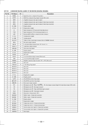
... U.CLOCK) Not used (Connected to ground) Power supply +5 V To tuner latch To tuner data To tuner clock PLL data in Auto stop input Stereo input Not used (Connected to ground) Not used (Connected to ground) Ground (Connected to ground) Not used (Connected to ground) TH Protector input...) Hardware standby (Connected to power supply +5 V) MD2 (To MCU MD2) MD1 (Connect to power supply) MD0 (To MCU MD0) Reset (Connected to MB90553 U.RESET) Ground (Connected to ground) External ceramic filter 16MHz is connected to this terminal External ceramic filter 16MHz is connected to this terminal Power supply...
... U.CLOCK) Not used (Connected to ground) Power supply +5 V To tuner latch To tuner data To tuner clock PLL data in Auto stop input Stereo input Not used (Connected to ground) Not used (Connected to ground) Ground (Connected to ground) Not used (Connected to ground) TH Protector input...) Hardware standby (Connected to power supply +5 V) MD2 (To MCU MD2) MD1 (Connect to power supply) MD0 (To MCU MD0) Reset (Connected to MB90553 U.RESET) Ground (Connected to ground) External ceramic filter 16MHz is connected to this terminal External ceramic filter 16MHz is connected to this terminal Power supply...
Service Manual
Page 32
... serial control register if P/S = "L" (Connected to ground) MCKO clock frequency select pin "L": MCLK, "H": MCLK/2. If the state of P/S, M/S, CAD0-1 changes, then the AK4526 must be reset by PD. I 30 LIN+ I 23 LOUT3 O 24 ROUT3 O 25 LOUT2 O 26 ROUT2 O 27 LOUT1 O 28 ROUT1 O 29 LIN- Pin Name I/O 1 SDOS I I 2...if P/S = "L" (Connected to ground) Master clock output pin (Not used) Digital power supply pin Digital ground pin Power-down & reset pin When "L", the AK4526 is enabled. (Connected to ground) Input clock select 1 pin (Connected to ground) Input clock select 0 pin...
... serial control register if P/S = "L" (Connected to ground) MCKO clock frequency select pin "L": MCLK, "H": MCLK/2. If the state of P/S, M/S, CAD0-1 changes, then the AK4526 must be reset by PD. I 30 LIN+ I 23 LOUT3 O 24 ROUT3 O 25 LOUT2 O 26 ROUT2 O 27 LOUT1 O 28 ROUT1 O 29 LIN- Pin Name I/O 1 SDOS I I 2...if P/S = "L" (Connected to ground) Master clock output pin (Not used) Digital power supply pin Digital ground pin Power-down & reset pin When "L", the AK4526 is enabled. (Connected to ground) Input clock select 1 pin (Connected to ground) Input clock select 0 pin...
Service Manual
Page 35
... IN 2 I 70 VIRSION IN 3 I 71 VIRSION IN 4 I 72 VIRSION IN 5 I 73 VIRSION OUT 1 O 74 VIRSION OUT 2 O 75 JOG-UP I 76 JOG-DOWN I 77 RESET I 78 FUNCTION UP I 79 FUNCTION DOWN I 80 - - 81 VSS - 82 X0 - 83 X1 - 84 VCC - 85 - - 86 - - 87 LED CLK I 88 LED DATA... RDS clock input RDS data input Volume up input. Speaker B signal input. POWER-KEY input. Not used (Connected to Ground) Reset output (Connected to MB90573 RESET) Slave request and data input (Connected to MB90573 SLV DATA/REQ) Master request output (Connected to MB90573 DISPMR) Master data output ...
... IN 2 I 70 VIRSION IN 3 I 71 VIRSION IN 4 I 72 VIRSION IN 5 I 73 VIRSION OUT 1 O 74 VIRSION OUT 2 O 75 JOG-UP I 76 JOG-DOWN I 77 RESET I 78 FUNCTION UP I 79 FUNCTION DOWN I 80 - - 81 VSS - 82 X0 - 83 X1 - 84 VCC - 85 - - 86 - - 87 LED CLK I 88 LED DATA... RDS clock input RDS data input Volume up input. Speaker B signal input. POWER-KEY input. Not used (Connected to Ground) Reset output (Connected to MB90573 RESET) Slave request and data input (Connected to MB90573 SLV DATA/REQ) Master request output (Connected to MB90573 DISPMR) Master data output ...
Service Manual
Page 36
... detect flag output. 33 BPSYNC O Non PCM sync detect flag output. 34 ERROR O Error mute output terminal 35 DO O Microprocessor I /F RECEIVER (DIGITAL BOARD) Pin No. IC1101 LC89055W DIGITAL AUDIO I /F. Pin Name I/O Description 1 DISEL I Input data select. (connected to ground.) ... - VDD - Digital power supply 31 D. When CCB/SUB is connected to ground) 6 D. Chip enable/latch input terminal 38 CLK I Microprocessor I Reset input. - 58 - Clock input terminal 39 XSEL I Xtal select. (Connected to +5V.) 40 MODE0 I Mode 0 input. (Connected to ground.)...
... detect flag output. 33 BPSYNC O Non PCM sync detect flag output. 34 ERROR O Error mute output terminal 35 DO O Microprocessor I /F RECEIVER (DIGITAL BOARD) Pin No. IC1101 LC89055W DIGITAL AUDIO I /F. Pin Name I/O Description 1 DISEL I Input data select. (connected to ground.) ... - VDD - Digital power supply 31 D. When CCB/SUB is connected to ground) 6 D. Chip enable/latch input terminal 38 CLK I Microprocessor I Reset input. - 58 - Clock input terminal 39 XSEL I Xtal select. (Connected to +5V.) 40 MODE0 I Mode 0 input. (Connected to ground.)...


