Service Manual
Page 4
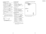
...your nearest Sony dealer. While recording from a digital component connected through the digital input connector, the digital connecting cable was not made properly. /Set the deck in order to standards. /Replace the disc, and repeat the recording procedure. This does not affect the recorded material....lighting is due to the following table in a stable place, and repeat the recording procedure. The inserted MD is record-protected. /Take out the MD, and close the record-protect tab (page 9.) The recording was unplugged or the digital component turned off. /Connect the cable or turn...
...your nearest Sony dealer. While recording from a digital component connected through the digital input connector, the digital connecting cable was not made properly. /Set the deck in order to standards. /Replace the disc, and repeat the recording procedure. This does not affect the recorded material....lighting is due to the following table in a stable place, and repeat the recording procedure. The inserted MD is record-protected. /Take out the MD, and close the record-protect tab (page 9.) The recording was unplugged or the digital component turned off. /Connect the cable or turn...
Service Manual
Page 16
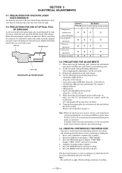
...power ¬ ¬ G ¬ adjustment 3. PRECAUTIONS FOR ADJUSTMENTS 1) When replacing the following tools and measuring devices. • Check Disc (MD) TDYS-1 (Parts No. 4-963-646-01) • Laser power meter LPM-8001 (Parts No. Rotate the AMS knob and display "CREC ...172; offset adjustment 2. After completing the adjustments, exit the test mode. 3) Perform the adjustments in the following describes how to create a continuous recorded data for checking BD board waveform (Parts No. : J-2501-124-A) 5) When observing several signals on page 4.) Note :When performing laser ...
...power ¬ ¬ G ¬ adjustment 3. PRECAUTIONS FOR ADJUSTMENTS 1) When replacing the following tools and measuring devices. • Check Disc (MD) TDYS-1 (Parts No. 4-963-646-01) • Laser power meter LPM-8001 (Parts No. Rotate the AMS knob and display "CREC ...172; offset adjustment 2. After completing the adjustments, exit the test mode. 3) Perform the adjustments in the following describes how to create a continuous recorded data for checking BD board waveform (Parts No. : J-2501-124-A) 5) When observing several signals on page 4.) Note :When performing laser ...
Service Manual
Page 18
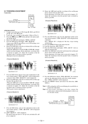
...the specified value is satisfied as much as possible. (Traverse Waveform) A VC B Specification A = B 17. Note 1 : MO reading data will be erased during if a recorded disc is satisfied as much as possible. (Traverse Waveform) A VC B Specification A = B 12. "EFB = MO-P". Connect an oscilloscope to CN110 pin 3 (TEO) and ...value. (When the AMS knob is rotated, the of adjustment to Note 1.) 3. Press the §EJECT button and remove the check disc (MD) TDYS-1. Adjust the waveform so that the waveform of the oscilloscope becomes the specified value. (When the AMS knob is rotated, the of "...
...the specified value is satisfied as much as possible. (Traverse Waveform) A VC B Specification A = B 17. Note 1 : MO reading data will be erased during if a recorded disc is satisfied as much as possible. (Traverse Waveform) A VC B Specification A = B 12. "EFB = MO-P". Connect an oscilloscope to CN110 pin 3 (TEO) and ...value. (When the AMS knob is rotated, the of adjustment to Note 1.) 3. Press the §EJECT button and remove the check disc (MD) TDYS-1. Adjust the waveform so that the waveform of the oscilloscope becomes the specified value. (When the AMS knob is rotated, the of "...
Service Manual
Page 19
... focal point position C is as shown in the above ), the focus bias adjustment may not have been carried out properly. Load a check disc (MD) TDYS-1. 2. Press the YES button twice and display "CPLAY MID". 4. Press the YES button and display " / b = ". FOCUS BIAS ...bias and check the focus tolerance amount. Press the YES button and display " / a = ". in the following figure using the average vale. 5-8. Creating Continuously Recorded Disc".). 2. Press the YES button and display " / c = ". 11. Rotate the AMS knob and display "CPLAY MODE". 3. Note 1 : The relation...
... focal point position C is as shown in the above ), the focus bias adjustment may not have been carried out properly. Load a check disc (MD) TDYS-1. 2. Press the YES button twice and display "CPLAY MID". 4. Press the YES button and display " / b = ". FOCUS BIAS ...bias and check the focus tolerance amount. Press the YES button and display " / a = ". in the following figure using the average vale. 5-8. Creating Continuously Recorded Disc".). 2. Press the YES button and display " / c = ". 11. Rotate the AMS knob and display "CPLAY MODE". 3. Note 1 : The relation...
Service Manual
Page 20
..., S685 - 688 LDON WRPWR MOD SDA SCL LIMIT REFLECT PROTECT CHUCK IN PACK OUT PB P REC P M903 LOADING MOTOR M LOAD-IN LOAD-OUT XRST - 22 - MDS-JE320 6-1. TRK+ FSC+ FSC-
..., S685 - 688 LDON WRPWR MOD SDA SCL LIMIT REFLECT PROTECT CHUCK IN PACK OUT PB P REC P M903 LOADING MOTOR M LOAD-IN LOAD-OUT XRST - 22 - MDS-JE320 6-1. TRK+ FSC+ FSC-
Service Manual
Page 21
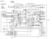
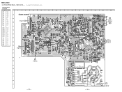
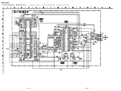
MAIN Section - MDS-JE320 - DOWN 12 2 9 8 POWER ON/OFF SW Q307, 308 +6V 1 +6V REG IC303 3 3 +B -B 7 -6V 3 -6V REG IC304 2 -32V 3 -32V REG IC310 1 RECT D309, 310 RECT ...
MAIN Section - MDS-JE320 - DOWN 12 2 9 8 POWER ON/OFF SW Q307, 308 +6V 1 +6V REG IC303 3 3 +B -B 7 -6V 3 -6V REG IC304 2 -32V 3 -32V REG IC310 1 RECT D309, 310 RECT ...
Service Manual
Page 22
... waveforms are taken with a VOM (Input impedance 10 MΩ). Replace only with respect to normal production tolerances. • Waveforms are dc with part number specified. MDS-JE320 6-2. or dotted line with mark !
... waveforms are taken with a VOM (Input impedance 10 MΩ). Replace only with respect to normal production tolerances. • Waveforms are dc with part number specified. MDS-JE320 6-2. or dotted line with mark !
Service Manual
Page 23
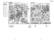
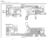
Printed Wiring Board - BD Section - • See page 25 for Circuit Boards Location. • Semiconductor Location Ref. Location D101 E-3 D181 C-9 D183 C-9 IC101 F-14 IC103 B-15 IC121 D-12 IC122 C-4 IC123 E-10 IC124 F-12 IC152 B-12 IC171 F-9 IC181 D-9 IC192 G-6 Q101 C-14 Q102 B-15 Q103 B-14 Q104 B-14 Q162 B-14 Q163 B-15 Q180 D-6 Q181 B-9 Q182 B-9 (Page 45) 16 (Page 33) MDS-JE320 (Page 33) - 27 - - 28 - No. 6-3.
Printed Wiring Board - BD Section - • See page 25 for Circuit Boards Location. • Semiconductor Location Ref. Location D101 E-3 D181 C-9 D183 C-9 IC101 F-14 IC103 B-15 IC121 D-12 IC122 C-4 IC123 E-10 IC124 F-12 IC152 B-12 IC171 F-9 IC181 D-9 IC192 G-6 Q101 C-14 Q102 B-15 Q103 B-14 Q104 B-14 Q162 B-14 Q163 B-15 Q180 D-6 Q181 B-9 Q182 B-9 (Page 45) 16 (Page 33) MDS-JE320 (Page 33) - 27 - - 28 - No. 6-3.
Service Manual
Page 24
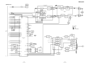
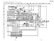
MDS-JE320 6-4. BD Section (1/2)- • See page 26 for Waveforms. • See page 49 for IC Block Diagrams. • See page 54 for IC Pin Functions. 16 (Page 31) - 29 - (Page 32) - 30 - Schematic Diagram -
MDS-JE320 6-4. BD Section (1/2)- • See page 26 for Waveforms. • See page 49 for IC Block Diagrams. • See page 54 for IC Pin Functions. 16 (Page 31) - 29 - (Page 32) - 30 - Schematic Diagram -
Service Manual
Page 25
BD Section (2/2) - • See page 26 for Waveforms. • See page 49 for IC Block Diagrams. • See page 54 for IC Pin Functions. (Page 29) (Page 30) MDS-JE320 BR24C01AF 16 (Page 36) (Page 47) (Page 35) - 31 - - 32 - 6-5. Schematic Diagram -
BD Section (2/2) - • See page 26 for Waveforms. • See page 49 for IC Block Diagrams. • See page 54 for IC Pin Functions. (Page 29) (Page 30) MDS-JE320 BR24C01AF 16 (Page 36) (Page 47) (Page 35) - 31 - - 32 - 6-5. Schematic Diagram -
Service Manual
Page 26
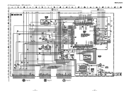
MDS-JE320 6-6. Printed Wiring Board - No. Main Section - • See page 25 for Circuit Boards Location. • Semiconductor Location Ref. Location 1 2 3 D301 G-11 D302 G-11 D303 G-...
MDS-JE320 6-6. Printed Wiring Board - No. Main Section - • See page 25 for Circuit Boards Location. • Semiconductor Location Ref. Location 1 2 3 D301 G-11 D302 G-11 D303 G-...

Service Manual
Page 27
Schematic Diagram - Main Section (1/3) - • See page 26 for Waveforms • See page 54 for IC Pin Functions. 6-7. MDS-JE320 (PAGE 32) - 35 - (PAGE 31) - 36 -
Schematic Diagram - Main Section (1/3) - • See page 26 for Waveforms • See page 54 for IC Pin Functions. 6-7. MDS-JE320 (PAGE 32) - 35 - (PAGE 31) - 36 -
Service Manual
Page 28
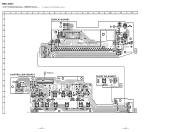
Main Section (2/3) - • See page 26 for Waveforms. • See page 49 for IC Block Diagrams. • See page 54 for IC Pin Functions. - 37 - - 38 - MDS-JE320 6-8. Schematic Diagram -
Main Section (2/3) - • See page 26 for Waveforms. • See page 49 for IC Block Diagrams. • See page 54 for IC Pin Functions. - 37 - - 38 - MDS-JE320 6-8. Schematic Diagram -
Service Manual
Page 29
Main Section (3/3) - • See page 49 for IC Block Diagram. MDS-JE320 (PAGE 44) - 39 - - 40 - Schematic Diagram - 6-9.
Main Section (3/3) - • See page 49 for IC Block Diagram. MDS-JE320 (PAGE 44) - 39 - - 40 - Schematic Diagram - 6-9.
Service Manual
Page 30
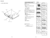
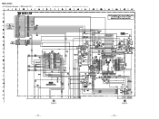
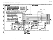
MDS-JE320 6-10. Printed Wiring Board - DISPLAY Section - • See page 25 for Circuit Boards Location. 1 2 3 4 5 6 7 8 9 A DISPLAY BOARD B C FLUORESCENT INDICATOR TUBE D 10 11 12 E E S764 1 3 21 1-661-891- (21) E F CONTROL (SW) BOARD REC LEVEL G H INPUT DIGITAL ANALOG C (PAGE 33) S762 DISPLAY/CHAR S774 S775 AMS (PUSH ENTER) 5 4 1 3 EJECT SW BOARD 1 S776 EJECT 3 CN705 21 1-661-893- (21) 1 3 I S771 S772 S780 S781 S752 S751 REC YES NO/EDIT 16 21 1-661-890- (21) - 41 - - 42 -
MDS-JE320 6-10. Printed Wiring Board - DISPLAY Section - • See page 25 for Circuit Boards Location. 1 2 3 4 5 6 7 8 9 A DISPLAY BOARD B C FLUORESCENT INDICATOR TUBE D 10 11 12 E E S764 1 3 21 1-661-891- (21) E F CONTROL (SW) BOARD REC LEVEL G H INPUT DIGITAL ANALOG C (PAGE 33) S762 DISPLAY/CHAR S774 S775 AMS (PUSH ENTER) 5 4 1 3 EJECT SW BOARD 1 S776 EJECT 3 CN705 21 1-661-893- (21) 1 3 I S771 S772 S780 S781 S752 S751 REC YES NO/EDIT 16 21 1-661-890- (21) - 41 - - 42 -
Service Manual
Page 31
Schematic Diagram - DISPLAY Section - • See page 26 for Waveforms. - 43 - 6-11. MDS-JE320 (PAGE 39) - 44 -
Schematic Diagram - DISPLAY Section - • See page 26 for Waveforms. - 43 - 6-11. MDS-JE320 (PAGE 39) - 44 -
Service Manual
Page 32
Printed Wiring Board - MDS-JE320 6-12. Switch Section - • See page 25 for Circuit Boards Location. 1 2 3 4 5 6 7 8 9 10 11 12 13 A B C (Page 28) D E F G H I J 16 - 45 - - 46 -
Printed Wiring Board - MDS-JE320 6-12. Switch Section - • See page 25 for Circuit Boards Location. 1 2 3 4 5 6 7 8 9 10 11 12 13 A B C (Page 28) D E F G H I J 16 - 45 - - 46 -
Service Manual
Page 56
MDS-JE320 MAIN SW Ref. TR301 A-4672-133-A MOTOR ASSY, SLED A-4672-134-A MOTOR ASSY, LOADING 1-429-735-11 TRANSFORMER, POWER (US,CND) 1-431-426-21 ... la sécurité. Ne les remplacer que par une pièce portant le numéro spécifié. 9-922-894-11 Sony Corporation Home A&V Products Company - 72 - 98F1664-1 Printed in Japan ©1998.6 Published by mark ! R363 R366 R367 R378 R383 Part No. No. Part No. Description...
MDS-JE320 MAIN SW Ref. TR301 A-4672-133-A MOTOR ASSY, SLED A-4672-134-A MOTOR ASSY, LOADING 1-429-735-11 TRANSFORMER, POWER (US,CND) 1-431-426-21 ... la sécurité. Ne les remplacer que par une pièce portant le numéro spécifié. 9-922-894-11 Sony Corporation Home A&V Products Company - 72 - 98F1664-1 Printed in Japan ©1998.6 Published by mark ! R363 R366 R367 R378 R383 Part No. No. Part No. Description...