Programmer Manual
Page 1
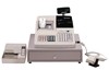
PROGRAM (PGM2/PGM1) MODE 17 CHAPTER 3. SERVICE (SRV) MODE 1 CHAPTER 2. The contents are subject to be used SHARP CORPORATION for after sales service only. OP X/Z, X1/Z1, X2/Z2 MODE 44 This document has been published to change without notice. ELECTRONIC CASH REGISTER MODEL ER-A450T (For "U" & "A" version) SRV KEY : LKGIM7113BHZZ PRINTER : PR-45M CONTENTS CHAPTER 1.
PROGRAM (PGM2/PGM1) MODE 17 CHAPTER 3. SERVICE (SRV) MODE 1 CHAPTER 2. The contents are subject to be used SHARP CORPORATION for after sales service only. OP X/Z, X1/Z1, X2/Z2 MODE 44 This document has been published to change without notice. ELECTRONIC CASH REGISTER MODEL ER-A450T (For "U" & "A" version) SRV KEY : LKGIM7113BHZZ PRINTER : PR-45M CONTENTS CHAPTER 1.
Service Manual
Page 1
... these parts with " " are subject to be used SHARP CORPORATION for maintaining the safety of the set . WHEN THE MODE SWITCH IS IN THE OFF POSITION, VOLTAGE IS STILL SUPPLIED TO THE ENTIRE MACHINE. DOWN LOAD FUNCTION 6-1 CHAPTER 7. SERVICE MANUAL ELECTRONIC CASH REGISTER MODEL ER-A450T SRV Key : LKGIM7113RCZZ PRINTER : PR-45M ("U" and "A" version...
... these parts with " " are subject to be used SHARP CORPORATION for maintaining the safety of the set . WHEN THE MODE SWITCH IS IN THE OFF POSITION, VOLTAGE IS STILL SUPPLIED TO THE ENTIRE MACHINE. DOWN LOAD FUNCTION 6-1 CHAPTER 7. SERVICE MANUAL ELECTRONIC CASH REGISTER MODEL ER-A450T SRV Key : LKGIM7113RCZZ PRINTER : PR-45M ("U" and "A" version...
Service Manual
Page 14
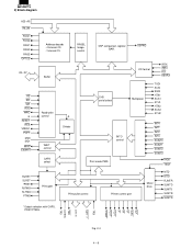
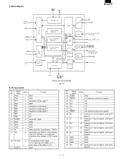
...; RESET RES VRESC POFF MD0 MD1 WAIT EXWAIT RJRST SLRST *PRST RJTMG SLTMG PTMG Address decode External CS Internal CS RASEL Image control SSP comparison register BAR.
...; RESET RES VRESC POFF MD0 MD1 WAIT EXWAIT RJRST SLRST *PRST RJTMG SLTMG PTMG Address decode External CS Internal CS RASEL Image control SSP comparison register BAR.
Service Manual
Page 19
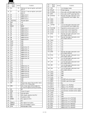
.... 16 O Thermalhead CLOCK signal SO is outputted at the edge of I Ä O, and is taken at the edge of o Ä I /O Data bus 4: Internal register, print buffer data IO - GND I /F UNIT CLOCK GEN. 3) Block diagram RD, WR A0~23 D0~7 WO WI INT INTI PHAI (Φ) INTERRUPT CIRCUIT HOST BUS... I /O Data bus 5: Internal register, print buffer data IO 4 - 11 GND - I Data return line, thermalhead -- name 1 GND 2 GND 3 ST1 4 GND 5 ST2 6 ST3 7 ST4 8 ST5 9 ST6 10 LATCH 11 ...
.... 16 O Thermalhead CLOCK signal SO is outputted at the edge of I Ä O, and is taken at the edge of o Ä I /O Data bus 4: Internal register, print buffer data IO - GND I /F UNIT CLOCK GEN. 3) Block diagram RD, WR A0~23 D0~7 WO WI INT INTI PHAI (Φ) INTERRUPT CIRCUIT HOST BUS... I /O Data bus 5: Internal register, print buffer data IO 4 - 11 GND - I Data return line, thermalhead -- name 1 GND 2 GND 3 ST1 4 GND 5 ST2 6 ST3 7 ST4 8 ST5 9 ST6 10 LATCH 11 ...
Service Manual
Page 20
...feed pulse motor common power control signal (Nu) - GND - Signal name In/Out Function 34 D6 I/O Data bus 6: Internal register, print buffer data IO 35 D7 I/O Data bus 7: Internal register, print buffer data IO 36 A0 I Address bus 0 37 A1 I Address bus 1 38 A2 I Journal motor connector sensor signal... 14 for PB-RAM O Address 13 for PB-RAM 4 - 12 D7 tri-state buffer 73 WR I Write strobe signal: Write enable into the internal register and the print buffer. 74 AS I AS 75 POF I Power off signal 76 INT O Interrupt signal 77 WO O Wait request signal to CPU 80 ...
...feed pulse motor common power control signal (Nu) - GND - Signal name In/Out Function 34 D6 I/O Data bus 6: Internal register, print buffer data IO 35 D7 I/O Data bus 7: Internal register, print buffer data IO 36 A0 I Address bus 0 37 A1 I Address bus 1 38 A2 I Journal motor connector sensor signal... 14 for PB-RAM O Address 13 for PB-RAM 4 - 12 D7 tri-state buffer 73 WR I Write strobe signal: Write enable into the internal register and the print buffer. 74 AS I AS 75 POF I Power off signal 76 INT O Interrupt signal 77 WO O Wait request signal to CPU 80 ...
Service Manual
Page 24
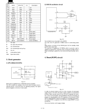
... of power off and power supply failure of the current program and immediately executes the power-off program to save the data in the CPU registers in most cases. 2) CKDC8 oscillation circuit 40 X2 CKDC 8 41 X1 37 XT2 38 XT1 HD404728A91FS C106 18P X1 4.19MHz 1 2 3 R164 330K X2 32.768KHz... 143 144 145 146 147 148 149 150 151 152 153 154 155 156 157 158 159 160 I ID IS ISU IO 3S ON6 Name ER-A770 I/O VCC VCC GND GND /CSD VCC IS TRNDTD NC O /DTRD NC O /RTSD NC O RCVDTD GND IS /CTSD GND IS /DSRD GND IS TRNRDYD NC...
... of power off and power supply failure of the current program and immediately executes the power-off program to save the data in the CPU registers in most cases. 2) CKDC8 oscillation circuit 40 X2 CKDC 8 41 X1 37 XT2 38 XT1 HD404728A91FS C106 18P X1 4.19MHz 1 2 3 R164 330K X2 32.768KHz... 143 144 145 146 147 148 149 150 151 152 153 154 155 156 157 158 159 160 I ID IS ISU IO 3S ON6 Name ER-A770 I/O VCC VCC GND GND /CSD VCC IS TRNDTD NC O /DTRD NC O /RTSD NC O RCVDTD GND IS /CTSD GND IS /DSRD GND IS TRNRDYD NC...
Service Manual
Page 25
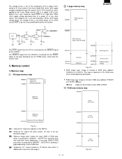
... a power off situation. ROM area memory map C00000H ROS1 (512K Byte) C00000H ROM area (3M byte) FFFFFFH Expansion I/O area (1M byte) Fig. 5-1 ( 1) "Internal I/O" means the registers in the H8/510. ( 2) "External I/O" means the base system I/O area to be formed in supply, 6.8V is supplied to the (+) pin, therefore, signal POFF is...
... a power off situation. ROM area memory map C00000H ROS1 (512K Byte) C00000H ROM area (3M byte) FFFFFFH Expansion I/O area (1M byte) Fig. 5-1 ( 1) "Internal I/O" means the registers in the H8/510. ( 2) "External I/O" means the base system I/O area to be formed in supply, 6.8V is supplied to the (+) pin, therefore, signal POFF is...
Service Manual
Page 26
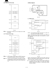
...signal is the base signal for initializing.) : For 0 page image area, selection between RAS2 and RAS3 can bemade with the control register. Note used in the ER-A445P. (Not used) Access is performed with two RAM chip select signals, RAS2 and RAS3. RAM control Address A23~A14 200000H~3FFFFFH... 1C0000H~1DFFFFH Address decorder 008000H~ 00F7FFH *1 1E0000H~1FFFFFH RAS3 RAS1 RAS2 DOI D Q Control register S8F CK R RESET MPCA7 Fig. 5-8 ...
...signal is the base signal for initializing.) : For 0 page image area, selection between RAS2 and RAS3 can bemade with the control register. Note used in the ER-A445P. (Not used) Access is performed with two RAM chip select signals, RAS2 and RAS3. RAM control Address A23~A14 200000H~3FFFFFH... 1C0000H~1DFFFFH Address decorder 008000H~ 00F7FFH *1 1E0000H~1FFFFFH RAS3 RAS1 RAS2 DOI D Q Control register S8F CK R RESET MPCA7 Fig. 5-8 ...

Service Manual
Page 27
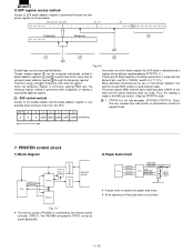
... bits 2 Intermediate bits Don't care for implementing the Special Service Preset(SSP). (Block diagram) NMI SSPRQ As the address detection system, the break address register comparison system is performed without shifting. The corresponding area is composed of ROS1 and ROS2. 4 - 19 FFFF00 7 0 H 1 1 2 2 3...~ D7 BAR 0 BAR N REGCS Decode Fig. 6-1 MPCA7 Comparator O Coincide N Coincide SSPRQ (NMI) SPE (Enable register) 2) SSP register The break address register (BAR) is performed through the direct address of the break address are assigned to , , and . SSP circuit 1)...
... bits 2 Intermediate bits Don't care for implementing the Special Service Preset(SSP). (Block diagram) NMI SSPRQ As the address detection system, the break address register comparison system is performed without shifting. The corresponding area is composed of ROS1 and ROS2. 4 - 19 FFFF00 7 0 H 1 1 2 2 3...~ D7 BAR 0 BAR N REGCS Decode Fig. 6-1 MPCA7 Comparator O Coincide N Coincide SSPRQ (NMI) SPE (Enable register) 2) SSP register The break address register (BAR) is performed through the direct address of the break address are assigned to , , and . SSP circuit 1)...
Service Manual
Page 28
... are read as binary data. Therefore any unnecessary read as binary data by the thermal printer controller (TPRC1). 3) SSP register access method Access to SSP break address register is performed through the temporary register. Therefore, set and to them from the CPU. bit 7 6 5 4 3 2 1 0 0 0 0 CMP4 CMP3 ...A pulse motor is used by FFFFFFH read.) 1: FFFFFFH is read access in the NMI sub routine. (Clear by BAR sets, the following register setting is performed after completion of setting of the pulse motor is as follows: 4 - 20 The break signals (NMI) and the above ...
... are read as binary data. Therefore any unnecessary read as binary data by the thermal printer controller (TPRC1). 3) SSP register access method Access to SSP break address register is performed through the temporary register. Therefore, set and to them from the CPU. bit 7 6 5 4 3 2 1 0 0 0 0 CMP4 CMP3 ...A pulse motor is used by FFFFFFH read.) 1: FFFFFFH is read access in the NMI sub routine. (Clear by BAR sets, the following register setting is performed after completion of setting of the pulse motor is as follows: 4 - 20 The break signals (NMI) and the above ...
Dealer Knowledge Book
Page 1
...or transmitted, in any means, electronic, mechanical, recording, or otherwise, without notice. Introduction - ER-A450 Set up - PC Setup for the ER-02FD 14 8. Converting Images for the Logo Converter Utility 8 5. Microsoft and Windows are subject to... ...1 2. Preliminary draft Dealer Knowledge Book I'm also here to the ER-A450T 11 7. MODEL ER-A450T LOGOCONV.exe Logo Converter Utility Contents Category Pg. 1. SIO Function ...7 4. Error Code Descriptions 16 9. Designs and specifications are either registered trademarks or trademarks of Sharp Corporation.
...or transmitted, in any means, electronic, mechanical, recording, or otherwise, without notice. Introduction - ER-A450 Set up - PC Setup for the ER-02FD 14 8. Converting Images for the Logo Converter Utility 8 5. Microsoft and Windows are subject to... ...1 2. Preliminary draft Dealer Knowledge Book I'm also here to the ER-A450T 11 7. MODEL ER-A450T LOGOCONV.exe Logo Converter Utility Contents Category Pg. 1. SIO Function ...7 4. Error Code Descriptions 16 9. Designs and specifications are either registered trademarks or trademarks of Sharp Corporation.


