
Data Sheet
Page 2
..., COPYRIGHT OR OTHER INTELLECTUAL PROPERTY RIGHT. Designers must not rely on which processors support Intel® 64 or consult with your system vendor for conflicts or incompatibilities arising from published specifications. The Intel® Core™ i7 Processor Extreme Edition and Intel® Core™ i7 Processor may contain design defects or errors known as errata which may make changes...
..., COPYRIGHT OR OTHER INTELLECTUAL PROPERTY RIGHT. Designers must not rely on which processors support Intel® 64 or consult with your system vendor for conflicts or incompatibilities arising from published specifications. The Intel® Core™ i7 Processor Extreme Edition and Intel® Core™ i7 Processor may contain design defects or errors known as errata which may make changes...
Data Sheet
Page 3
...SAD_INTERLEAVE_LIST_0, SAD_INTERLEAVE_LIST_1 SAD_INTERLEAVE_LIST_2, SAD_INTERLEAVE_LIST_3 SAD_INTERLEAVE_LIST_4, SAD_INTERLEAVE_LIST_5 SAD_INTERLEAVE_LIST_6, SAD_INTERLEAVE_LIST_7 47 2.7 Intel QPI Link Registers 48 2.7.1 QPI_QPILCL_L0, QPI_QPILCL_L1 48 2.8 Integrated Memory Controller..., TAD_DRAM_RULE_3 TAD_DRAM_RULE_4, TAD_DRAM_RULE_5 TAD_DRAM_RULE_6, TAD_DRAM_RULE_7 58 Datasheet 3 Contents 1 Introduction ...11 1.1 Terminology ...11 1.1.1 Processor Terminology 11 1.2 References ...13 2 Register Description 15 2.1 Register Terminology 15 2.2 Platform Configuration Structure 16 ...
...SAD_INTERLEAVE_LIST_0, SAD_INTERLEAVE_LIST_1 SAD_INTERLEAVE_LIST_2, SAD_INTERLEAVE_LIST_3 SAD_INTERLEAVE_LIST_4, SAD_INTERLEAVE_LIST_5 SAD_INTERLEAVE_LIST_6, SAD_INTERLEAVE_LIST_7 47 2.7 Intel QPI Link Registers 48 2.7.1 QPI_QPILCL_L0, QPI_QPILCL_L1 48 2.8 Integrated Memory Controller..., TAD_DRAM_RULE_3 TAD_DRAM_RULE_4, TAD_DRAM_RULE_5 TAD_DRAM_RULE_6, TAD_DRAM_RULE_7 58 Datasheet 3 Contents 1 Introduction ...11 1.1 Terminology ...11 1.1.1 Processor Terminology 11 1.2 References ...13 2 Register Description 15 2.1 Register Terminology 15 2.2 Platform Configuration Structure 16 ...
Data Sheet
Page 8
Tables 1-1 References...13 2-1 Functions Specifically Handled by the Processor 18 2-2 Device 0, Function 0: Generic Non-core Registers 19 2-3 Device 0, Function 1: System Address Decoder Registers 20 2-4 Device 2, Function 0: Intel QPI Link 0 Registers 21 2-5 Device 2, Function 1: Intel QPI Physical 0 Registers 22 2-6 Device 3, Function 0: Integrated Memory Controller Registers 23 2-7 Device 3, Function 1: Target Address Decoder Registers 24 2-8 Device 4, Function 0: Integrated...
Tables 1-1 References...13 2-1 Functions Specifically Handled by the Processor 18 2-2 Device 0, Function 0: Generic Non-core Registers 19 2-3 Device 0, Function 1: System Address Decoder Registers 20 2-4 Device 2, Function 0: Intel QPI Link 0 Registers 21 2-5 Device 2, Function 1: Intel QPI Physical 0 Registers 22 2-6 Device 3, Function 0: Integrated Memory Controller Registers 23 2-7 Device 3, Function 1: Target Address Decoder Registers 24 2-8 Device 4, Function 0: Integrated...
Data Sheet
Page 11
... system. Introduction 1 Introduction Note: 1.1 1.1.1 The Intel® Core™ i7 processor Extreme Edition and Intel® Core™ i7 processor are intended for some classes of viruses or worms that is low, a reset has been requested. In this document the Intel® Core™ i7 processor Extreme Edition and Intel® Core™ i7 processor will be marked as "the processor." Processor features vary by component and include...
... system. Introduction 1 Introduction Note: 1.1 1.1.1 The Intel® Core™ i7 processor Extreme Edition and Intel® Core™ i7 processor are intended for some classes of viruses or worms that is low, a reset has been requested. In this document the Intel® Core™ i7 processor Extreme Edition and Intel® Core™ i7 processor will be marked as "the processor." Processor features vary by component and include...
Data Sheet
Page 12
.... Refers to any supply voltages, have any clocks. • Intel® Core™ i7 processor Extreme Edition and Intel® Core™ i7 processor - Under these conditions, processor lands should not be found at http://developer.intel.com/technology/intel64/. • Intel® QuickPath Interconnect - Further details on the top side of Intel 64. The portion of the package. A component of the...
.... Refers to any supply voltages, have any clocks. • Intel® Core™ i7 processor Extreme Edition and Intel® Core™ i7 processor - Under these conditions, processor lands should not be found at http://developer.intel.com/technology/intel64/. • Intel® QuickPath Interconnect - Further details on the top side of Intel 64. The portion of the package. A component of the...
Data Sheet
Page 13
Introduction • Unit Interval (UI) - References Document Intel® Core™ i7 Processor Extreme Edition and Intel® Core™ i7 Processor Specification Update Intel® Core™ i7 Processor Extreme Edition and Intel® Core™ i7 Processor Datasheet, Volume 1 Intel® Core™ i7 Processor Extreme Edition and Intel® Core™ i7 Processor and LGA1366 Socket Thermal and Mechanical Design Guide Intel® 64 and IA-32 Intel® Architecture Software Developer's Manual •...
Introduction • Unit Interval (UI) - References Document Intel® Core™ i7 Processor Extreme Edition and Intel® Core™ i7 Processor Specification Update Intel® Core™ i7 Processor Extreme Edition and Intel® Core™ i7 Processor Datasheet, Volume 1 Intel® Core™ i7 Processor Extreme Edition and Intel® Core™ i7 Processor and LGA1366 Socket Thermal and Mechanical Design Guide Intel® 64 and IA-32 Intel® Architecture Software Developer's Manual •...
Data Sheet
Page 15
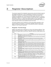
...Base Specification, Revision 1.1. A register bit with this attribute can be read . The write causes some hardware event to all processors. This attribute is applied to this bit. All multi-byte numeric fields use "little-endian" ordering (i.e., lower addresses contain ...to a 2 bit field, and only one will get cleared after power up. Register Description 2 Register Description 2.1 i The processor supports PCI configuration space accesses using the mechanism denoted as Configuration Mechanism in the PCI specification as defined in the PCI Local Bus...
...Base Specification, Revision 1.1. A register bit with this attribute can be read . The write causes some hardware event to all processors. This attribute is applied to this bit. All multi-byte numeric fields use "little-endian" ordering (i.e., lower addresses contain ...to a 2 bit field, and only one will get cleared after power up. Register Description 2 Register Description 2.1 i The processor supports PCI configuration space accesses using the mechanism denoted as Configuration Mechanism in the PCI specification as defined in the PCI Local Bus...
Data Sheet
Page 16
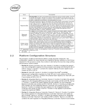
..." or unchanged by the max bus range setting and processor socket number. • Device 0: Generic processor non-core. Note that contains a reserved bit is responsible for the Configuration Address (CONFIG_ADDRESS) register. Registers that are marked as devices residing on the PCI bus assigned for Intel QPI Link 0 and resides at DID of the system...
..." or unchanged by the max bus range setting and processor socket number. • Device 0: Generic processor non-core. Note that contains a reserved bit is responsible for the Configuration Address (CONFIG_ADDRESS) register. Registers that are marked as devices residing on the PCI bus assigned for Intel QPI Link 0 and resides at DID of the system...
Data Sheet
Page 17
...Processor Component Register Group Intel QuickPath Architecture Generic Non-core Registers Intel QuickPath Architecture System Address Decoder Intel QPI Link 0 Intel QPI Physical 0 Integrated Memory Controller Registers Integrated Memory Controller Target Address Decoder Integrated Memory Controller RAS Registers Integrated Memory Controller Test Registers Integrated Memory Controller Channel 0 Control Processor... Notes: 1. Functions Specifically Handled by the max bus range setting and processor socket number. Device 5, Function 3 contains the thermal control registers for ...
...Processor Component Register Group Intel QuickPath Architecture Generic Non-core Registers Intel QuickPath Architecture System Address Decoder Intel QPI Link 0 Intel QPI Physical 0 Integrated Memory Controller Registers Integrated Memory Controller Target Address Decoder Integrated Memory Controller RAS Registers Integrated Memory Controller Test Registers Integrated Memory Controller Channel 0 Control Processor... Notes: 1. Functions Specifically Handled by the max bus range setting and processor socket number. Device 5, Function 3 contains the thermal control registers for ...
Data Sheet
Page 36
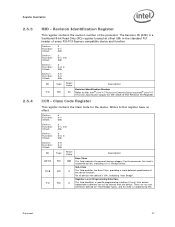
...this register have no effect. Device Identification Register This 16-bit register combined with the Device Identification Register uniquely identifies the manufacturer of the processor. 36 Datasheet Device: Function: Offset: 0 0-1 02h Device: Function: Offset: 2 0-1, 4-5 02h Device: Function: Offset: 3 0-2,...function for the DID of each function of the function within the processor. VID - Vendor Identification Register The VID Register contains the vendor identification number. Writes to Intel. Register Description 2.5 Note: 2.5.1 2.5.2 PCI Standard Registers These registers...
...this register have no effect. Device Identification Register This 16-bit register combined with the Device Identification Register uniquely identifies the manufacturer of the processor. 36 Datasheet Device: Function: Offset: 0 0-1 02h Device: Function: Offset: 2 0-1, 4-5 02h Device: Function: Offset: 3 0-2,...function for the DID of each function of the function within the processor. VID - Vendor Identification Register The VID Register contains the vendor identification number. Writes to Intel. Register Description 2.5 Note: 2.5.1 2.5.2 PCI Standard Registers These registers...
Data Sheet
Page 37
...: 4-6 0-3 08h Bit Type Reset Value Description Revision Identification Number 7:0 RO 0h Refer to the Intel® Core™ i7 Processor Extreme Edition and Intel® Core™ i7 Processor Specification Update for the value of every PCI/PCI Express compatible device and function. Class Code Register ... field indicates the general device category. CCR - Register Description 2.5.3 2.5.4 RID - There are no effect. For the processor, this field is hardwired to this field is hardwired to interact with the device. Register-Level Programming Interface This field ...
...: 4-6 0-3 08h Bit Type Reset Value Description Revision Identification Number 7:0 RO 0h Refer to the Intel® Core™ i7 Processor Extreme Edition and Intel® Core™ i7 Processor Specification Update for the value of every PCI/PCI Express compatible device and function. Class Code Register ... field indicates the general device category. CCR - Register Description 2.5.3 2.5.4 RID - There are no effect. For the processor, this field is hardwired to this field is hardwired to interact with the device. Register-Level Programming Interface This field ...
Data Sheet
Page 38
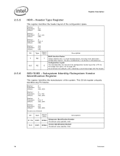
... configuration layouts. Register Description 2.5.5 2.5.6 HDR - Configuration Layout 0 This field identifies the format of the configuration header layout for devices in the processor. This 32-bit register uniquely identifies any PCI device. SID/SVID - Device: Function: Offset: 0 0-1 2Ch, 2Eh Device: Function: Offset...Type RWO RWO Reset Value Description Subsystem Identification Number 8086h The default value specifies Intel Vendor Identification Number 8086h The default value specifies Intel. 38 Datasheet This bit is hardwired to 1 for a PCI-toPCI bridge ...
... configuration layouts. Register Description 2.5.5 2.5.6 HDR - Configuration Layout 0 This field identifies the format of the configuration header layout for devices in the processor. This 32-bit register uniquely identifies any PCI device. SID/SVID - Device: Function: Offset: 0 0-1 2Ch, 2Eh Device: Function: Offset...Type RWO RWO Reset Value Description Subsystem Identification Number 8086h The default value specifies Intel Vendor Identification Number 8086h The default value specifies Intel. 38 Datasheet This bit is hardwired to 1 for a PCI-toPCI bridge ...
Data Sheet
Page 47
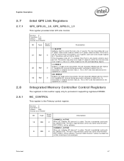
... is required to determine if a transmitter is controlled (set by software only. Register Description 2.7 2.7.1 2.8 2.8.1 Intel QPI Link Registers QPI_QPILCL_L0, QPI_QPILCL_L1 This register provides Intel QPI Link Control. This link transmitter bit is set /reset) 9 RW 0 by software. The master may ...the receive 0 L0s capability bit received during parameter exchange to be ANDed with an ACK or NACK. This bit is allowed to processors supporting registered DIMMs. MC_CONTROL This register is NOT a bit that determines the capability of L1 is enabled, then there is active...
... is required to determine if a transmitter is controlled (set by software only. Register Description 2.7 2.7.1 2.8 2.8.1 Intel QPI Link Registers QPI_QPILCL_L0, QPI_QPILCL_L1 This register provides Intel QPI Link Control. This link transmitter bit is set /reset) 9 RW 0 by software. The master may ...the receive 0 L0s capability bit received during parameter exchange to be ANDed with an ACK or NACK. This bit is allowed to processors supporting registered DIMMs. MC_CONTROL This register is NOT a bit that determines the capability of L1 is enabled, then there is active...
Data Sheet
Page 63
This bit applies only to processors supporting registered DIMMs. WR_VALID. 0 Indicates current command is for a read CAS. Bit is cleared by a DDR3CMD write. RD_VALID. 0 Indicates current command is for the DRAM ...
This bit applies only to processors supporting registered DIMMs. WR_VALID. 0 Indicates current command is for a read CAS. Bit is cleared by a DDR3CMD write. RD_VALID. 0 Indicates current command is for the DRAM ...
Data Sheet
Page 96
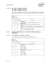
... to 40h, the value read from the corresponding in this register are frozen. 0 RW 0 LOCK. Rank 2 virtual temperature. 0 RANK1. ASSERTION and DEASSERTION fields in the processor datasheet (i.e., what an assertion of the pin does). Rank 0 virtual temperature. 2.13.10 MC_DDR_THERM_COMMAND0 MC_DDR_THERM_COMMAND1 MC_DDR_THERM_COMMAND2 This register contains the command portion of each rank...
... to 40h, the value read from the corresponding in this register are frozen. 0 RW 0 LOCK. Rank 2 virtual temperature. 0 RANK1. ASSERTION and DEASSERTION fields in the processor datasheet (i.e., what an assertion of the pin does). Rank 0 virtual temperature. 2.13.10 MC_DDR_THERM_COMMAND0 MC_DDR_THERM_COMMAND1 MC_DDR_THERM_COMMAND2 This register contains the command portion of each rank...
Data Sheet
Page 97
... of the pin, and may be several clocks out of Qclk. Write-1-to -clear. 1 RO 0 DEASSERTION. Device: 3 Function: 4 Offset: 50h Access as described in the processor datasheet (i.e., what is asserted 2.14 2.14.1 Integrated Memory Controller Miscellaneous Registers MC_DIMM_CLK_RATIO_STATUS This register contains status information about DIMM clock ratio. Current ratio of date...
... of the pin, and may be several clocks out of Qclk. Write-1-to -clear. 1 RO 0 DEASSERTION. Device: 3 Function: 4 Offset: 50h Access as described in the processor datasheet (i.e., what is asserted 2.14 2.14.1 Integrated Memory Controller Miscellaneous Registers MC_DIMM_CLK_RATIO_STATUS This register contains status information about DIMM clock ratio. Current ratio of date...

