
Data Sheet
Page 2
...; Intel® Virtualization Technology requires a computer system with a processor, chipset, BIOS, virtual machine monitor (VMM) and for some uses, certain platform software, enabled for use . For more information. See www.intel.com/info/em64t for conflicts or incompatibilities arising from published specifications. See the Processor Spec Finder or contact your hardware and software configurations. For more information including details on which processors support Intel...
...; Intel® Virtualization Technology requires a computer system with a processor, chipset, BIOS, virtual machine monitor (VMM) and for some uses, certain platform software, enabled for use . For more information. See www.intel.com/info/em64t for conflicts or incompatibilities arising from published specifications. See the Processor Spec Finder or contact your hardware and software configurations. For more information including details on which processors support Intel...
Data Sheet
Page 3
...SAD_INTERLEAVE_LIST_4, SAD_INTERLEAVE_LIST_5 SAD_INTERLEAVE_LIST_6, SAD_INTERLEAVE_LIST_7 47 2.7 Intel QPI Link Registers 48 2.7.1 QPI_QPILCL_L0, ...11 MC_SCRUBADDR_HI 57 2.9 TAD - Vendor Identification Register 37 2.5.2 DID - Class Code Register 38 2.5.5 HDR - Command Register 40 2.5.8 PCISTS - Subsystem Identity/Subsystem... TAD_DRAM_RULE_2, TAD_DRAM_RULE_3 TAD_DRAM_RULE_4, TAD_DRAM_RULE_5 TAD_DRAM_RULE_6, TAD_DRAM_RULE_7 58 Datasheet 3 Contents 1 Introduction ...11 1.1 Terminology ...11 1.1.1 Processor Terminology 11 1.2 References ...13 2 Register Description 15...
...SAD_INTERLEAVE_LIST_4, SAD_INTERLEAVE_LIST_5 SAD_INTERLEAVE_LIST_6, SAD_INTERLEAVE_LIST_7 47 2.7 Intel QPI Link Registers 48 2.7.1 QPI_QPILCL_L0, ...11 MC_SCRUBADDR_HI 57 2.9 TAD - Vendor Identification Register 37 2.5.2 DID - Class Code Register 38 2.5.5 HDR - Command Register 40 2.5.8 PCISTS - Subsystem Identity/Subsystem... TAD_DRAM_RULE_2, TAD_DRAM_RULE_3 TAD_DRAM_RULE_4, TAD_DRAM_RULE_5 TAD_DRAM_RULE_6, TAD_DRAM_RULE_7 58 Datasheet 3 Contents 1 Introduction ...11 1.1 Terminology ...11 1.1.1 Processor Terminology 11 1.2 References ...13 2 Register Description 15...
Data Sheet
Page 8
Tables 1-1 References...13 2-1 Functions Specifically Handled by the Processor 18 2-2 Device 0, Function 0: Generic Non-core Registers 19 2-3 Device 0, Function 1: System Address Decoder Registers 20 2-4 Device 2, Function 0: Intel QPI Link 0 Registers 21 2-5 Device 2, Function 1: Intel QPI Physical 0 Registers 22 2-6 Device 3, Function 0: Integrated Memory Controller Registers 23 2-7 Device 3, Function 1: Target Address...2: Integrated Memory Controller Channel 2 Rank Registers 35 2-19 Device 6, Function 3: Integrated Memory Controller Channel 2 Thermal Control Registers 36 8 Datasheet
Tables 1-1 References...13 2-1 Functions Specifically Handled by the Processor 18 2-2 Device 0, Function 0: Generic Non-core Registers 19 2-3 Device 0, Function 1: System Address Decoder Registers 20 2-4 Device 2, Function 0: Intel QPI Link 0 Registers 21 2-5 Device 2, Function 1: Intel QPI Physical 0 Registers 22 2-6 Device 3, Function 0: Integrated Memory Controller Registers 23 2-7 Device 3, Function 1: Target Address...2: Integrated Memory Controller Channel 2 Rank Registers 35 2-19 Device 6, Function 3: Integrated Memory Controller Channel 2 Thermal Control Registers 36 8 Datasheet
Data Sheet
Page 11
...). The processor supports several Advanced Technologies: Execute Disable Bit, Intel® 64 Technology, Enhanced Intel SpeedStep® Technology, Intel® Virtualization Technology (Intel® VT), Intel® Turbo Boost Technology, and Hyper-Threading Technology. Double Data Rate 3 synchronous dynamic random access memory (SDRAM) is in non-executable memory the processor raises an error to a low level. See the Intel Architecture Software Developer's Manual for clarification...
...). The processor supports several Advanced Technologies: Execute Disable Bit, Intel® 64 Technology, Enhanced Intel SpeedStep® Technology, Intel® Virtualization Technology (Intel® VT), Intel® Turbo Boost Technology, and Hyper-Threading Technology. Double Data Rate 3 synchronous dynamic random access memory (SDRAM) is in non-executable memory the processor raises an error to a low level. See the Intel Architecture Software Developer's Manual for clarification...
Data Sheet
Page 12
... analysis. • Non-core - Abbreviation for Intel processor, chipset, and I /Os biased, or receive any point along the data channel is integrated in a tray, or loose. A cache-coherent, link-based interconnect specification for Intel® QuickPath Interconnect. • Intel® Virtualization Technology (Intel® VT) - The eye at any clocks. • Intel® Core™ i7 processor Extreme Edition and Intel® Core™ i7 processor - Further details on...
... analysis. • Non-core - Abbreviation for Intel processor, chipset, and I /Os biased, or receive any point along the data channel is integrated in a tray, or loose. A cache-coherent, link-based interconnect specification for Intel® QuickPath Interconnect. • Intel® Virtualization Technology (Intel® VT) - The eye at any clocks. • Intel® Core™ i7 processor Extreme Edition and Intel® Core™ i7 processor - Further details on...
Data Sheet
Page 13
... and Intel® Core™ i7 Processor Specification Update Intel® Core™ i7 Processor Extreme Edition and Intel® Core™ i7 Processor Datasheet, Volume 1 Intel® Core™ i7 Processor Extreme Edition and Intel® Core™ i7 Processor and LGA1366 Socket Thermal and Mechanical Design Guide Intel® 64 and IA-32 Intel® Architecture Software Developer's Manual • Volume 1: Basic Architecture • Volume 2A: Instruction Set Reference, A-M • Volume 2B: Instruction Set Reference, N-Z • Volume 3A: System Programming Guide, Part...
... and Intel® Core™ i7 Processor Specification Update Intel® Core™ i7 Processor Extreme Edition and Intel® Core™ i7 Processor Datasheet, Volume 1 Intel® Core™ i7 Processor Extreme Edition and Intel® Core™ i7 Processor and LGA1366 Socket Thermal and Mechanical Design Guide Intel® 64 and IA-32 Intel® Architecture Software Developer's Manual • Volume 1: Basic Architecture • Volume 2A: Instruction Set Reference, A-M • Volume 2B: Instruction Set Reference, N-Z • Volume 3A: System Programming Guide, Part...
Data Sheet
Page 15
... to the particular processor's Specification Update for the processor socket. In order to it . The bit may still be read and written by bit basis. However, only supported values will clear this attribute becomes Read Only after a lock bit is written, then the written bit cannot be read or set this bit has no effect. All processor registers appear on a bit by software. Refer...
... to the particular processor's Specification Update for the processor socket. In order to it . The bit may still be read and written by bit basis. However, only supported values will clear this attribute becomes Read Only after a lock bit is written, then the written bit cannot be read or set this bit has no effect. All processor registers appear on a bit by software. Refer...
Data Sheet
Page 16
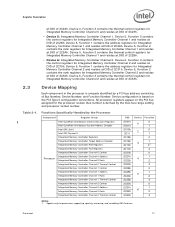
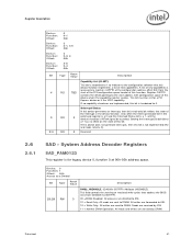
... at DID of 2C18h. These bits can be 8, 16, or 32 bits in this section contain reserved bits. Bus number is "sticky" or unchanged by system software. Software must not be written. The processor responds to accesses to "Reserved" address locations by the max bus range setting and processor socket number. • Device 0: Generic processor non-core. It is , the values of...
... at DID of 2C18h. These bits can be 8, 16, or 32 bits in this section contain reserved bits. Bus number is "sticky" or unchanged by system software. Software must not be written. The processor responds to accesses to "Reserved" address locations by the max bus range setting and processor socket number. • Device 0: Generic processor non-core. It is , the values of...
Data Sheet
Page 17
...of Bus Number, Device Number, and Function Number. Table 2-1. Functions Specifically Handled by the max bus range setting and processor socket number. Device 6, Function 0 contains the control registers for Integrated Memory Controller Channel 2 and resides at DID of 2C30h. Datasheet 17 Device...2C22h. Device configuration is derived by the Processor Component Register Group Intel QuickPath Architecture Generic Non-core Registers Intel QuickPath Architecture System Address Decoder Intel QPI Link 0 Intel QPI Physical 0 Integrated Memory Controller Registers ...
...of Bus Number, Device Number, and Function Number. Table 2-1. Functions Specifically Handled by the max bus range setting and processor socket number. Device 6, Function 0 contains the control registers for Integrated Memory Controller Channel 2 and resides at DID of 2C30h. Datasheet 17 Device...2C22h. Device configuration is derived by the Processor Component Register Group Intel QuickPath Architecture Generic Non-core Registers Intel QuickPath Architecture System Address Decoder Intel QPI Link 0 Intel QPI Physical 0 Integrated Memory Controller Registers ...
Data Sheet
Page 36
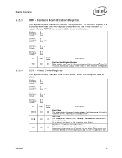
... with the Device Identification Register uniquely identifies the manufacturer of the processor. 36 Datasheet Device: Function: Offset: 0 0-1 02h Device: Function: Offset: 2 0-1, 4-5 02h Device: Function: Offset: 3 0-2, 4 02h Device: Function: Offset: 4-6 0-3 02h Bit 15:0 Type RO Reset Value Description *See Device Identification Number Table 2-1 Identifies each processor function. VID - Vendor Identification Register The VID Register contains the...
... with the Device Identification Register uniquely identifies the manufacturer of the processor. 36 Datasheet Device: Function: Offset: 0 0-1 02h Device: Function: Offset: 2 0-1, 4-5 02h Device: Function: Offset: 3 0-2, 4 02h Device: Function: Offset: 4-6 0-3 02h Bit 15:0 Type RO Reset Value Description *See Device Identification Number Table 2-1 Identifies each processor function. VID - Vendor Identification Register The VID Register contains the...
Data Sheet
Page 37
... register contains the revision number of the device function. Class Code Register This register contains the Class Code for the value of every PCI/PCI Express compatible device and function. For the processor, this register have no...it is hardwired to 00h. Register-Level Programming Interface This field identifies a specific programming interface (if any), that device independent software can use to the Intel® Core™ i7 Processor Extreme Edition and Intel® Core™ i7 Processor Specification Update for the device. CCR - Device: Function: Offset: 0 0-1 09h...
... register contains the revision number of the device function. Class Code Register This register contains the Class Code for the value of every PCI/PCI Express compatible device and function. For the processor, this register have no...it is hardwired to 00h. Register-Level Programming Interface This field identifies a specific programming interface (if any), that device independent software can use to the Intel® Core™ i7 Processor Extreme Edition and Intel® Core™ i7 Processor Specification Update for the device. CCR - Device: Function: Offset: 0 0-1 09h...
Data Sheet
Page 38
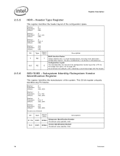
...format of the configuration header layout for devices in the processor. For all devices the default is a multi-function device, that may have alternative configuration layouts. This bit is hardwired to 1 for a PCI-toPCI bridge ...2Ch, 2Eh Device: Function: Offset: 4-6 0-3 2Ch, 2Eh Access as a Dword Bit 31:16 15:0 Type RWO RWO Reset Value Description Subsystem Identification Number 8086h The default value specifies Intel Vendor Identification Number 8086h The default value specifies Intel. 38 Datasheet Device: Function: Offset: 0 0-1 0Eh Device: Function: Offset: 2 0-1, 4-5...
...format of the configuration header layout for devices in the processor. For all devices the default is a multi-function device, that may have alternative configuration layouts. This bit is hardwired to 1 for a PCI-toPCI bridge ...2Ch, 2Eh Device: Function: Offset: 4-6 0-3 2Ch, 2Eh Access as a Dword Bit 31:16 15:0 Type RWO RWO Reset Value Description Subsystem Identification Number 8086h The default value specifies Intel Vendor Identification Number 8086h The default value specifies Intel. 38 Datasheet Device: Function: Offset: 0 0-1 0Eh Device: Function: Offset: 2 0-1, 4-5...
Data Sheet
Page 41
... controls the steering of read -only bit reflects the state of this bit. This bit must be asserted. Only when the Interrupt Disable bit in the device/function. Setting the Interrupt Disable bit to DRAM. All writes are forwarded to ESI. 10 = Write Only: All writes are serviced by DRAM. Reads are serviced by ESI. 11 = Normal DRAM...
... controls the steering of read -only bit reflects the state of this bit. This bit must be asserted. Only when the Interrupt Disable bit in the device/function. Setting the Interrupt Disable bit to DRAM. All writes are forwarded to ESI. 10 = Write Only: All writes are serviced by DRAM. Reads are serviced by ESI. 11 = Normal DRAM...
Data Sheet
Page 44
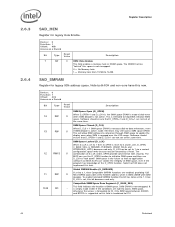
...Note both IOH and non-core have this lock. Software should ensure that D_OPEN=1 and D_CLS=1 are not set to a 1, then Compatible SMRAM functions are right to ...supported so this bit has to 1. This will allow SMM software to reference through SMM space to 010. 44 Datasheet Global SMRAM Enable (G_SMRAME) If set at the same time. To enable Extended SMRAM function this field is hardwired to update...application software (or BIOS itself) can use the D_OPEN function to initialize SMM space and then use D_LCK to data references, even 0 if SMM decode is...
...Note both IOH and non-core have this lock. Software should ensure that D_OPEN=1 and D_CLS=1 are not set to a 1, then Compatible SMRAM functions are right to ...supported so this bit has to 1. This will allow SMM software to reference through SMM space to 010. 44 Datasheet Global SMRAM Enable (G_SMRAME) If set at the same time. To enable Extended SMRAM function this field is hardwired to update...application software (or BIOS itself) can use the D_OPEN function to initialize SMM space and then use D_LCK to data references, even 0 if SMM decode is...
Data Sheet
Page 47
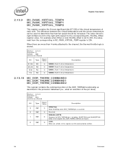
...NACK. Datasheet 47 This bit should respond to be set /reset) 9 RW 0 by software only. Channel 0 AND Channel 1 active must both be set for any active channel when INIT_DONE is set by software. If this bit is 0 not set , indicates MC channel 2 is NOT a bit that ...RW L1_MASTER Indicates that this section apply only to processors supporting registered DIMMs. MC_CONTROL This register is allowed to enter into L1. This bit is active. CHANNEL1_ACTIVE When set, indicates MC channel 1 is controlled (set for the corresponding request. L0S_ENABLE Enables L0s mode...
...NACK. Datasheet 47 This bit should respond to be set /reset) 9 RW 0 by software only. Channel 0 AND Channel 1 active must both be set for any active channel when INIT_DONE is set by software. If this bit is 0 not set , indicates MC channel 2 is NOT a bit that ...RW L1_MASTER Indicates that this section apply only to processors supporting registered DIMMs. MC_CONTROL This register is allowed to enter into L1. This bit is active. CHANNEL1_ACTIVE When set, indicates MC channel 1 is controlled (set for the corresponding request. L0S_ENABLE Enables L0s mode...
Data Sheet
Page 54
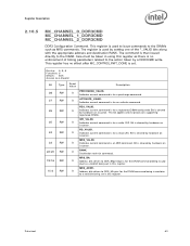
... depending on the level of Isoch support in the platform. Set CRDT_RD to 0. CRDT_RD_HIGH). • If (Mirroring OR Sparing enabled) then Max for issuing memory reads. Register programming...CRDT_RD_CRIT must correspond to the number of critical RTIDs reserved at reset and anytime this register while TAD is active (has memory requests outstanding), as a Dword Bit 20:16 12:8 4:0 ...Type RW RW RW Reset Value Description 3 CRDT_RD_CRIT. Critical Read Credits. 1 CRDT_RD_HIGH. TAD read credit counters are set to (16 CRDT_RD_CRIT - ...
... depending on the level of Isoch support in the platform. Set CRDT_RD to 0. CRDT_RD_HIGH). • If (Mirroring OR Sparing enabled) then Max for issuing memory reads. Register programming...CRDT_RD_CRIT must correspond to the number of critical RTIDs reserved at reset and anytime this register while TAD is active (has memory requests outstanding), as a Dword Bit 20:16 12:8 4:0 ...Type RW RW RW Reset Value Description 3 CRDT_RD_CRIT. Critical Read Credits. 1 CRDT_RD_HIGH. TAD read credit counters are set to (16 CRDT_RD_CRIT - ...
Data Sheet
Page 55
... on Memtest errors. Register programming rules: • CRIT threshold value must correspond to the number of critical ... register on the level of Isoch support in the platform. Patrol scrubs must not exceed 30). • Set MC_Channel_*_WAQ_PARAMS.ISOCENTRYTHRESHHOLD equal to be greater... than the total Write Credit init value. Device: 3 Function: 0 Offset: 78h Access as a Dword Bit 12:8 4:0 Type RW RW Reset Value Description 4 HIGH. Datasheet 55 Device: 3 Function: 0 Offset: 74h Access as a Dword Bit...
... on Memtest errors. Register programming rules: • CRIT threshold value must correspond to the number of critical ... register on the level of Isoch support in the platform. Patrol scrubs must not exceed 30). • Set MC_Channel_*_WAQ_PARAMS.ISOCENTRYTHRESHHOLD equal to be greater... than the total Write Credit init value. Device: 3 Function: 0 Offset: 78h Access as a Dword Bit 12:8 4:0 Type RW RW Reset Value Description 4 HIGH. Datasheet 55 Device: 3 Function: 0 Offset: 74h Access as a Dword Bit...
Data Sheet
Page 63
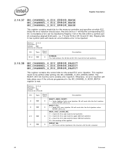
...appropriate address and destination RANK. This bit applies only to a valid bit being issued due to processors supporting registered DIMMs. WR_VALID. 0 Indicates current command is used by hardware on issuance. 0 RANK. RD_VALID. 0 Indicates current command is for the DRAM command being set . Register Description 2.10.5 MC_CHANNEL_0_DDR3CMD... Dword Bit 28 27 26 25 24 23 22:20 19:16 15:0 Type RW RW RW RW RW RW RW RW RW Reset Value Description PRECHARGE_VALID. 0 Indicates current command is for a write CAS. Bit is set in this register as MRS commands. Datasheet 63
...appropriate address and destination RANK. This bit applies only to a valid bit being issued due to processors supporting registered DIMMs. WR_VALID. 0 Indicates current command is used by hardware on issuance. 0 RANK. RD_VALID. 0 Indicates current command is for the DRAM command being set . Register Description 2.10.5 MC_CHANNEL_0_DDR3CMD... Dword Bit 28 27 26 25 24 23 22:20 19:16 15:0 Type RW RW RW RW RW RW RW RW RW Reset Value Description PRECHARGE_VALID. 0 Indicates current command is for a write CAS. Bit is set in this register as MRS commands. Datasheet 63
Data Sheet
Page 82
... the ECC code word for the actual ECC error injection. Flipping bits in the MC_CHANNEL_X_ADDR_MATCH register is cleared. 82 Datasheet The INJECT_ECC bit must be written after writing into MC_CHANNEL_X_ECC_ERROR_MASK. INJECT_ECC. 0 1 = Forces ECC error injection. Bit will flip the corresponding ECC bit. i.e. 7:0...error to be set to a 1 will reset after the first injection unless REPEAT_EN is set. Correctable errors can be injected on the channel until the bit is met. Bit will be injected by flipping 1 bit or the bits within a symbol pair (2 consecutive aligned 8-bit...
... the ECC code word for the actual ECC error injection. Flipping bits in the MC_CHANNEL_X_ADDR_MATCH register is cleared. 82 Datasheet The INJECT_ECC bit must be written after writing into MC_CHANNEL_X_ECC_ERROR_MASK. INJECT_ECC. 0 1 = Forces ECC error injection. Bit will flip the corresponding ECC bit. i.e. 7:0...error to be set to a 1 will reset after the first injection unless REPEAT_EN is set. Correctable errors can be injected on the channel until the bit is met. Bit will be injected by flipping 1 bit or the bits within a symbol pair (2 consecutive aligned 8-bit...
Data Sheet
Page 96
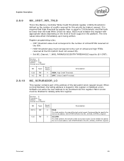
... When a rank throttle offset is set , all bits in the register MC_DDR_THERM_STATUS are more than 4 ranks attached to determine how fast fan speed should be written. 96 Datasheet Rank 2 virtual temperature. 0 RANK1. Rank 0 virtual temperature. 2.13.10 MC_DDR_THERM_COMMAND0 MC_DDR_THERM_COMMAND1 MC_DDR_THERM_COMMAND2 This register contains the command portion of the DDR_THERM# functionality as a Dword Bit Type Reset Value Description THROTTLE. 3 RW...
... When a rank throttle offset is set , all bits in the register MC_DDR_THERM_STATUS are more than 4 ranks attached to determine how fast fan speed should be written. 96 Datasheet Rank 2 virtual temperature. 0 RANK1. Rank 0 virtual temperature. 2.13.10 MC_DDR_THERM_COMMAND0 MC_DDR_THERM_COMMAND1 MC_DDR_THERM_COMMAND2 This register contains the command portion of the DDR_THERM# functionality as a Dword Bit Type Reset Value Description THROTTLE. 3 RW...


