
Hard Drive Specifications
Page 5
...3.1 Formatted Capacity 9 3.2 Data Sheet 9 3.3 Cylinder Allocation 10 3.4 Performance Characteristics 10 3.4.1 Command overhead 11 3.4.2 Mechanical Positioning 11 3.4.3 Drive Ready Time 13 3.4.4 Spindle Stop Time 13 3.4.5 Data Transfer Speed 13 3.4.6 Buffering Operation (Lookahead/Write Cache 14 3.4.7 Throughput 15 4.0... SCSI Bus Terminator 27 6.1.4 Hot Plug / Unplug 27 6.1.5 SCSI Bus Electrical Characteristics 28 6.1.6 Auxiliary Connector on 68-pin Model 29 6.2 Option Jumper Block 30 6.2.1 Jumper Signal Description 32 6.2.2 Shipping Default 35 6.3 LED Circuit 36 6.3.1 50-Pin...
...3.1 Formatted Capacity 9 3.2 Data Sheet 9 3.3 Cylinder Allocation 10 3.4 Performance Characteristics 10 3.4.1 Command overhead 11 3.4.2 Mechanical Positioning 11 3.4.3 Drive Ready Time 13 3.4.4 Spindle Stop Time 13 3.4.5 Data Transfer Speed 13 3.4.6 Buffering Operation (Lookahead/Write Cache 14 3.4.7 Throughput 15 4.0... SCSI Bus Terminator 27 6.1.4 Hot Plug / Unplug 27 6.1.5 SCSI Bus Electrical Characteristics 28 6.1.6 Auxiliary Connector on 68-pin Model 29 6.2 Option Jumper Block 30 6.2.1 Jumper Signal Description 32 6.2.2 Shipping Default 35 6.3 LED Circuit 36 6.3.1 50-Pin...
Hard Drive Specifications
Page 6
...Model 38 6.4 Environment 39 6.5 Cooling Requirements 40 6.6 DC Power Requirements 41 6.6.1 Start Up Current 42 6.7 Reliability 43 6.7.1 Contact Start Stop (CSS 43 6.7.2 Data Reliability 43 6.7.3 Seek/ID Mis-compare Errors 43 6.7.4 Equipment Errors 43 6.7.5 Failure Prediction ( PFA / S.M.A.R.T 43 6.7.6 Automatic Drive....6 Secondary Circuit Protection 59 6.14 Packaging 59 Part 2. EVPD = 0 72 7.6.2 Inquiry Data Format - EVPD = 1 - of DDRS-3xxxx SCSI Interface Specification 61 7.0 SCSI COMMAND SET 63 7.1 Flag and Link Bits 64 7.2 Abbreviations 65 7.3 Byte ordering conventions 65...
...Model 38 6.4 Environment 39 6.5 Cooling Requirements 40 6.6 DC Power Requirements 41 6.6.1 Start Up Current 42 6.7 Reliability 43 6.7.1 Contact Start Stop (CSS 43 6.7.2 Data Reliability 43 6.7.3 Seek/ID Mis-compare Errors 43 6.7.4 Equipment Errors 43 6.7.5 Failure Prediction ( PFA / S.M.A.R.T 43 6.7.6 Automatic Drive....6 Secondary Circuit Protection 59 6.14 Packaging 59 Part 2. EVPD = 0 72 7.6.2 Inquiry Data Format - EVPD = 1 - of DDRS-3xxxx SCSI Interface Specification 61 7.0 SCSI COMMAND SET 63 7.1 Flag and Link Bits 64 7.2 Abbreviations 65 7.3 Byte ordering conventions 65...

Hard Drive Specifications
Page 13
Closed loop actuator servo Dedicated head landing zone Automatic actuator lock Informational Exceptions Control Page of the drive Data capacity 9.1 GB and 4.5 GB | SE models, 50/68/80-pin | LVD models, 68/80-pin (capable to work also as PFA or S.M.A.R.T. 1.0 Outline of SCSI-3 support as SE) SCSI-2 Standard | SCSI-3 FAST-20 WIDE ( 40 Mbytes/... diagnostics Automatic Defect Reallocatio 7.5 msec seek time in read operation 7200rpm spindle rotation. function Note: PFA which means Predictive Failure Analysis is Trademark of IBM Corporation. © Copyright IBM Corp. 1997 3
Closed loop actuator servo Dedicated head landing zone Automatic actuator lock Informational Exceptions Control Page of the drive Data capacity 9.1 GB and 4.5 GB | SE models, 50/68/80-pin | LVD models, 68/80-pin (capable to work also as PFA or S.M.A.R.T. 1.0 Outline of SCSI-3 support as SE) SCSI-2 Standard | SCSI-3 FAST-20 WIDE ( 40 Mbytes/... diagnostics Automatic Defect Reallocatio 7.5 msec seek time in read operation 7200rpm spindle rotation. function Note: PFA which means Predictive Failure Analysis is Trademark of IBM Corporation. © Copyright IBM Corp. 1997 3

Hard Drive Specifications
Page 23
... transfer rate (Mbyte/sec) is categolized as operating, and Operating Shock criteria are applied until complete stop of the linear density recording. read, write) immediately. Drive Ready Time | Model | DDRS-39130 | DDRS-34560 Typical 15.5 [ sec] 10.5 [ sec] Max. 19.9 [ sec] 19.9 [ sec] Ready Power On The condition in which the...
... transfer rate (Mbyte/sec) is categolized as operating, and Operating Shock criteria are applied until complete stop of the linear density recording. read, write) immediately. Drive Ready Time | Model | DDRS-39130 | DDRS-34560 Typical 15.5 [ sec] 10.5 [ sec] Max. 19.9 [ sec] 19.9 [ sec] Ready Power On The condition in which the...

Hard Drive Specifications
Page 31
...of 50-pin and 68-pin models is shown in 6.1.1.5, "SCSI Signal Connector (80-pin SE)" on page 25 and 6.1.1.6, "SCSI Signal Connector (80-pin LVD)" on page 26. Pin 1 2 3 4 Figure 14. Power connector of 80-pin models comply with the ANSI SCSI"A" ...connector specifications. Connector of 50-pin models comply with SFF-8046 Revision 2.1. Power Connector Pin Assignments Voltage + 12 V GND GND + 5V © Copyright IBM Corp. 1997 21 6.0 Specification 6.1 Electrical Interface Specification 6.1.1 Connectors...
...of 50-pin and 68-pin models is shown in 6.1.1.5, "SCSI Signal Connector (80-pin SE)" on page 25 and 6.1.1.6, "SCSI Signal Connector (80-pin LVD)" on page 26. Pin 1 2 3 4 Figure 14. Power connector of 80-pin models comply with the ANSI SCSI"A" ...connector specifications. Connector of 50-pin models comply with SFF-8046 Revision 2.1. Power Connector Pin Assignments Voltage + 12 V GND GND + 5V © Copyright IBM Corp. 1997 21 6.0 Specification 6.1 Electrical Interface Specification 6.1.1 Connectors...

Hard Drive Specifications
Page 36
Table of DDRS-3xxxx of Signals | Connector | Contact | Number Signal Name | 01 12 Volt Charge | 02 12 Volt | 03 12 Volt | 04 12 Volt | 05 Reserved | 06 Reserved | ...,39,40,77,78,79,80 work as Logical O R with SFF-8046 Revision 2.1. | Figure 19. | 6.1.1.6 SCSI Signal Connector (80-pin LVD) | The 80-pin SCA-2 model uses an AMP connector which is compatible with jumper pins on Option Jumper Block. 26 OEM Spec.
Table of DDRS-3xxxx of Signals | Connector | Contact | Number Signal Name | 01 12 Volt Charge | 02 12 Volt | 03 12 Volt | 04 12 Volt | 05 Reserved | 06 Reserved | ...,39,40,77,78,79,80 work as Logical O R with SFF-8046 Revision 2.1. | Figure 19. | 6.1.1.6 SCSI Signal Connector (80-pin LVD) | The 80-pin SCA-2 model uses an AMP connector which is compatible with jumper pins on Option Jumper Block. 26 OEM Spec.

Hard Drive Specifications
Page 37
... between terminators shall be 1.5 meters when using from five to eight maximum capacitance devices. (ANSI SCSI-3 FAST-20 X3T10/1071D). | 6.1.2.2 LVD model | The maximum cumulative cable length when using LVD transcever must be 12 meter. The maximum cumulative signal path length between terminators shall be 3.0 meters...18 pins of the auxiliary connector on 68 SCSI pin models. It is also driven by installing a jumper between pins 13 and 14 of the jumper block, or connecting pins 9 and 10 of 68pin model) is provided by drive 5V supply through current limiter and shotky diode, and internal...
... between terminators shall be 1.5 meters when using from five to eight maximum capacitance devices. (ANSI SCSI-3 FAST-20 X3T10/1071D). | 6.1.2.2 LVD model | The maximum cumulative cable length when using LVD transcever must be 12 meter. The maximum cumulative signal path length between terminators shall be 3.0 meters...18 pins of the auxiliary connector on 68 SCSI pin models. It is also driven by installing a jumper between pins 13 and 14 of the jumper block, or connecting pins 9 and 10 of 68pin model) is provided by drive 5V supply through current limiter and shotky diode, and internal...

Hard Drive Specifications
Page 38
Logic Signal Levels | 6.1.5.2 LVD model | SCSI Bus Electrical Characteristics of DDRS-3xxxx of LVD models comply with ANSI SPI-2 T10 Project 1142D Revision | 19. 28 OEM Spec. Output High Voltage = High Impedanc Output Low Voltage = 0.5 V max./IO=48mA Figure 20. 6.1.5 SCSI Bus Electrical Characteristics | 6.1.5.1 SE model The interface logic signals has the following electrical specifications: Inputs : Outputs : Input High Voltage = 2.0 V min. Input Low Voltage = 0.8 V max.
Logic Signal Levels | 6.1.5.2 LVD model | SCSI Bus Electrical Characteristics of DDRS-3xxxx of LVD models comply with ANSI SPI-2 T10 Project 1142D Revision | 19. 28 OEM Spec. Output High Voltage = High Impedanc Output Low Voltage = 0.5 V max./IO=48mA Figure 20. 6.1.5 SCSI Bus Electrical Characteristics | 6.1.5.1 SE model The interface logic signals has the following electrical specifications: Inputs : Outputs : Input High Voltage = 2.0 V min. Input Low Voltage = 0.8 V max.

Hard Drive Specifications
Page 39
...be open. Pin #8 is for external LED cathod. | If pin #9 is valid only for SE model. | LVD model has no terminator. Pin #1,3,5,7 specify SCSI-ID as logical OR. 6.1.6 Auxiliary Connector on SE model, SCSI Terminator is enabled. | Enable SE SCSI Terminator +5V DAS3 DAS2 DAS1 DAS0 Pin#: 11 9 ...6 4 2 (Reserved) (Reserved) (Reserved) | Note: Pin #9 is tied-down to the ground is to the ground on 68-pin Model The 68-pin models contain Auxiliary Connector between power connector and 68-pin SCSI connector in addition to Option Jumper Block. Auxiliary Connector Specification 29 The...
...be open. Pin #8 is for external LED cathod. | If pin #9 is valid only for SE model. | LVD model has no terminator. Pin #1,3,5,7 specify SCSI-ID as logical OR. 6.1.6 Auxiliary Connector on SE model, SCSI Terminator is enabled. | Enable SE SCSI Terminator +5V DAS3 DAS2 DAS1 DAS0 Pin#: 11 9 ...6 4 2 (Reserved) (Reserved) (Reserved) | Note: Pin #9 is tied-down to the ground is to the ground on 68-pin Model The 68-pin models contain Auxiliary Connector between power connector and 68-pin SCSI connector in addition to Option Jumper Block. Auxiliary Connector Specification 29 The...

Hard Drive Specifications
Page 40
Some of DDRS-3xxxx Jumper Pins Note: The pin alocation is used to select the SCSI device ID, Auto spin up option ...SCSI parity option control. of the above items can be also controled through Auxiliary Connector as descrived in 6.1.6, "Auxiliary Connector on 68-pin Model" on page 29. These controls work as logical O R between Option Jumper Block and Auxiliary Connector. It also provides an external Light ... Enclosure Figure 21. 6.2 Option Jumper Block The 12 positions jumper block shown below is not compatible with previous IBM HDDs such as DPES-xxxxx, DALS-xxxxx. 30 OEM Spec.
Some of DDRS-3xxxx Jumper Pins Note: The pin alocation is used to select the SCSI device ID, Auto spin up option ...SCSI parity option control. of the above items can be also controled through Auxiliary Connector as descrived in 6.1.6, "Auxiliary Connector on 68-pin Model" on page 29. These controls work as logical O R between Option Jumper Block and Auxiliary Connector. It also provides an external Light ... Enclosure Figure 21. 6.2 Option Jumper Block The 12 positions jumper block shown below is not compatible with previous IBM HDDs such as DPES-xxxxx, DALS-xxxxx. 30 OEM Spec.
Hard Drive Specifications
Page 42
...If a shunt jumper is installed on 50/68-pin drive, the internal terminator on the drive works. 80-pin drive has not internal terminator. | 6.2.1.5 Position 6 on LVD models (Force SCSI Single-End Mode) | If a shunt jumper is installed, the drive is the most significant bit. DAS3 DAS2 DAS1 DAS0 ... 1 2 3 4 5 6< 7 8 9 10 11 12 13 14 15 Shipping default of 80 pin Shipping default of DDRS-3xxxx If a shunt jumper | is installed, the drive will spin up automatically after power on reset. 6.2.1 Jumper Signal Description Throughout this paragraph ON means a shunt jumper is installed and...
...If a shunt jumper is installed on 50/68-pin drive, the internal terminator on the drive works. 80-pin drive has not internal terminator. | 6.2.1.5 Position 6 on LVD models (Force SCSI Single-End Mode) | If a shunt jumper is installed, the drive is the most significant bit. DAS3 DAS2 DAS1 DAS0 ... 1 2 3 4 5 6< 7 8 9 10 11 12 13 14 15 Shipping default of 80 pin Shipping default of DDRS-3xxxx If a shunt jumper | is installed, the drive will spin up automatically after power on reset. 6.2.1 Jumper Signal Description Throughout this paragraph ON means a shunt jumper is installed and...

Hard Drive Specifications
Page 45
...set as shipping default on 80-pin models. | SCSI ID is set to #6 as shipping default on 50/68-pin models. | SCSI terminator is enabled as shipping default on SE 50/68-pin models. | Auto Spin up is enabled on all models. | Shipping Default Setting of SE 50... | 12 11 10 9 8 7 6 5 4 3 2 1 | | | oooooooooooo | | oooooooooooo | | | Shunt jumpers are installed at position 2,3,5 and 6 as shipping default of LVD 68-pin model Specification 35 No shunt jumper is installed on 80 pin model. | Figure 27. Default Jumper Setting of SE 50/68-pin | Shipping Default Setting on 80 pin...
...set as shipping default on 80-pin models. | SCSI ID is set to #6 as shipping default on 50/68-pin models. | SCSI terminator is enabled as shipping default on SE 50/68-pin models. | Auto Spin up is enabled on all models. | Shipping Default Setting of SE 50... | 12 11 10 9 8 7 6 5 4 3 2 1 | | | oooooooooooo | | oooooooooooo | | | Shunt jumpers are installed at position 2,3,5 and 6 as shipping default of LVD 68-pin model Specification 35 No shunt jumper is installed on 80 pin model. | Figure 27. Default Jumper Setting of SE 50/68-pin | Shipping Default Setting on 80 pin...
Hard Drive Specifications
Page 46
The schematics of the the jumper pins, the following pins can be used to drive LED. 68-Pin Model : Auxiliary Connector Pin #8 and #11. 80-Pin Model : SCA-2 Connector Pin #77 as shown in 6.3.3, "80-Pin Model" on each model are used to drive an external LED. 6.3 LED Circuit Jumper pin #1 and #2 are as follows. 6.3.1 50-Pin Model DDRS 39130 / DDRS 34560 50 Pin Model +5V o > < 620 Ohm > o Jumper Pin #1 for LED Anode o Jumper Pin #2 for LED Cathod / \ /// Figure 28. Instead of LED circuit on page 38. LED Circuit of DDRS-3xxxx of 50-Pin Model 36 OEM Spec.
The schematics of the the jumper pins, the following pins can be used to drive LED. 68-Pin Model : Auxiliary Connector Pin #8 and #11. 80-Pin Model : SCA-2 Connector Pin #77 as shown in 6.3.3, "80-Pin Model" on each model are used to drive an external LED. 6.3 LED Circuit Jumper pin #1 and #2 are as follows. 6.3.1 50-Pin Model DDRS 39130 / DDRS 34560 50 Pin Model +5V o > < 620 Ohm > o Jumper Pin #1 for LED Anode o Jumper Pin #2 for LED Cathod / \ /// Figure 28. Instead of LED circuit on page 38. LED Circuit of DDRS-3xxxx of 50-Pin Model 36 OEM Spec.

Hard Drive Specifications
Page 47
LED Circuit of Usage : at System Side : : : : : : o : : : : : \/ : \ / LED : : : : : : : : : : : : : : : : : o : : : Figure 29. 6.3.2 68-Pin Model DDRS 39130 / DDRS 34560 68 Pin Model : : : : 5V : o : Auxiliary : Connector Pin #11 o for LED Anode : : > : < 620 Ohm : > : : Jumper Pin #1 for LED Anode o : : : o / Jumper Pin #2 for LED Cathod \ : : > : < 150 Ohm : > : : Auxiliary : Connector Pin #8 /// o for LED Cathod : : : : Example of 68-Pin Model Specification 37
LED Circuit of Usage : at System Side : : : : : : o : : : : : \/ : \ / LED : : : : : : : : : : : : : : : : : o : : : Figure 29. 6.3.2 68-Pin Model DDRS 39130 / DDRS 34560 68 Pin Model : : : : 5V : o : Auxiliary : Connector Pin #11 o for LED Anode : : > : < 620 Ohm : > : : Jumper Pin #1 for LED Anode o : : : o / Jumper Pin #2 for LED Cathod \ : : > : < 150 Ohm : > : : Auxiliary : Connector Pin #8 /// o for LED Cathod : : : : Example of 68-Pin Model Specification 37
Hard Drive Specifications
Page 48
LED Circuit of DDRS-3xxxx of 80-Pin (SCA-2) Model 38 OEM Spec. 6.3.3 80-Pin Model DDRS 39130 / DDRS 34560 80 Pin (SCA 2) Model : : : : +5V +5V : o o : : : > > : 1K Ohm < < 620 Ohm : > > : : : : \/ : LED \ / : Jumper Pin #1 for LED Anode o : : : o / Jumper Pin #2 for LED Cathod \ : : : SCA 2 Connector Pin #77 /// o for LED Cathod : : : Example of Usage : at System Side : : : +5V : o : : : > : < 150 Ohm : > : : : : \/ : \ / LED : : : : : : : : : : : : : o : : : Figure 30.
LED Circuit of DDRS-3xxxx of 80-Pin (SCA-2) Model 38 OEM Spec. 6.3.3 80-Pin Model DDRS 39130 / DDRS 34560 80 Pin (SCA 2) Model : : : : +5V +5V : o o : : : > > : 1K Ohm < < 620 Ohm : > > : : : : \/ : LED \ / : Jumper Pin #1 for LED Anode o : : : o / Jumper Pin #2 for LED Cathod \ : : : SCA 2 Connector Pin #77 /// o for LED Cathod : : : Example of Usage : at System Side : : : +5V : o : : : > : < 150 Ohm : > : : : : \/ : \ / LED : : : : : : : : : : : : : o : : : Figure 30.

Hard Drive Specifications
Page 55
6.8 Mechanical Specifications 6.8.1 Outline 6.8.1.1 50-pin Model Figure 39. Outline of 50-pin Model Specification 45
6.8 Mechanical Specifications 6.8.1 Outline 6.8.1.1 50-pin Model Figure 39. Outline of 50-pin Model Specification 45

Hard Drive Specifications
Page 56
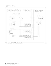
Outline of DDRS-3xxxx 6.8.1.2 68-pin Model Figure 40. of 68-pin Model 46 OEM Spec.
Outline of DDRS-3xxxx 6.8.1.2 68-pin Model Figure 40. of 68-pin Model 46 OEM Spec.

Hard Drive Specifications
Page 57
Outline of 80-pin Model Specification 47 6.8.1.3 80-pin Model Figure 41.
Outline of 80-pin Model Specification 47 6.8.1.3 80-pin Model Figure 41.

Hard Drive Specifications
Page 59
Interface Connector (50-pin Model) Specification 49 6.8.3 Interface Connector 6.8.3.1 50-pin Model Figure 44.
Interface Connector (50-pin Model) Specification 49 6.8.3 Interface Connector 6.8.3.1 50-pin Model Figure 44.

Hard Drive Specifications
Page 60
Interface Connector (68-pin Model) 50 OEM Spec. 6.8.3.2 68-pin Model Figure 45. of DDRS-3xxxx
Interface Connector (68-pin Model) 50 OEM Spec. 6.8.3.2 68-pin Model Figure 45. of DDRS-3xxxx
