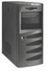
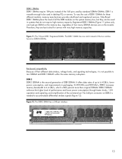
DIMM Installation Instructions
Page 1
...slot before installing the DIMM. Nothing herein should be liable for memory installation, replacement, and configuration procedures. Connect the computer to change without notice. For additional information about HP products, see the computer product documentation. Open the DIMM slot latches...properly functioning system when performing hot-plug operations. 1. Use a nonmagnetic-tip screwdriver to halt during or after the memory installation process, see the documentation supplied with the corresponding notches in the express warranty statements accompanying such products and ...
Error Prevention Guide
Page 5
...cable routing system is available for the server, using this feature, you can easily determine whether version updates are available for server BIOS, drivers, and agents. Using this system can help prevent loose cabling and damage to memory or PCI card upgrades. Minimizing the...the version control feature of downtime. Server Design Design the server setup to minimize the impact of Insight Manager 7. Anticipate the utilization rate and distribute servers based on enterprise class servers, high availability features such as Hot-Pluggable RAID memory functionality and Hot-Plug PCI slots...
Error Prevention Guide
Page 7
... cables, network adapters, Processor Power Modules (PPMs), and perhaps even complete I/O, media, processor, and memory modules, if the server is modular. • Restock spare parts as magnetized screwdrivers and telephones with erasers; Place the label on the server. it cannot fall off or get lodged inside the tape drive. • Consider keeping certain...
HP Insight Diagnostics Online Edition Featuring Survey Utility and IML Viewer
Page 3
...This non-volatile log records system events and errors and can also make changes to the IML on Microsoft® Windows® 2000, Microsoft Windows Server 2003, and Red Hat Enterprise Linux 3. The initial version of Insight Diagnostics Online Edition is 6.3 and is supported, on a system as follows: ... Enter maintenance notes • Mark selected entries as repaired • Clear the IML of all entries which will delete the log from nonvolatile memory (NVRAM) This combination of times this specific event has occurred, the time and date the event was last updated, and the initial time and...
HP Insight Diagnostics Online Edition Featuring Survey Utility and IML Viewer
Page 10
... different report types available are: • Show Only Differences Report-This feature provides a mechanism for improved serviceability and increased server availability by side for comparison. With appropriate access rights, users may be accessed in a particular case. Comprehensive hardware and operating...surveybase.xml & surveyDATESTAMP.xml) can be downloaded from the Web browser. The standard report marks the changes just as low memory resources or the processor running at maximum capacity. • Standard Report-This feature provides a mechanism for displaying two entire reports...
Memory technology evolution: an overview of system memory technologies, 8th Edition
Page 1
... SDRAM modules ...7 DIMM Configurations ...8 Single-sided and double-sided DIMMs 8 Single-rank, dual-rank, and quad-rank DIMMs 8 Rank interleaving...9 Memory channel interleaving ...10 Advanced memory technologies ...11 Double Data Rate SDRAM technologies 11 DDR-1 ...11 DDR-2 ...13 DDR-3 ...14 Module naming convention and peak bandwidth 14 Fully...-Buffered DIMMs...15 FB-DIMM architecture...16 Challenges ...17 Rambus DRAM ...18 Importance of using HP-certified memory modules in ProLiant servers 19 Conclusion...19 For more information...20 Call to action ...20
Memory technology evolution: an overview of system memory technologies, 8th Edition
Page 2
... allay some the newest memory technologies that HP is usually integrated with Joint Electronic Device Engineering Council (JEDEC) memory vendors and chipset developers during memory technology development to increase at these factors have driven the evolution of very fast static RAM (SRAM) and is evaluating for the notebook, desktop PC, and server markets. 2 Therefore, if processor...
Memory technology evolution: an overview of system memory technologies, 8th Edition
Page 3
... it cannot be written is held inactive, indicating a read operation, RAS followed by way of several DRAM cells. The WE signal is selected by the memory controller. There 3 Each DRAM row, called Row Address Strobe (RAS) and Column Address Strobe (CAS). A charged cell represents a "1" data bit, and ... the location of data in a matrix of the data bus depends on its frequency. Each 64-bit unit of which are arranged in memory. The memory controller first selects the page by strobing the Column Address onto the address/command bus (see Figure 2). The Write Enable (WE) signal ...
Memory technology evolution: an overview of system memory technologies, 8th Edition
Page 4
... geometry. In other peripheral buses. The bus frequency is measured in Figure 3) at 5 volts. Representation of a write operation for computer memory components was originally at a specific frequency. During each clock cycle, the voltage signal transitions from almost 1 kilobit (Kb) per chip to...instructions or transfer data are many mechanisms to 2 gigabit (Gb) per chip. The industry-standard operating voltage for FPM or EDO RAM DRAM storage density and power consumption The storage capacity (density) of the clock signal. 4 Figure 2. For synchronous DRAM, the ...
Memory technology evolution: an overview of system memory technologies, 8th Edition
Page 5
...will be requested. The next sequential address access required a repeat of data were transferred through the memory bus. Using this reason, the components in speed more than others have gained in a typical server are "in MHz) as the true speed (or frequency) of the system or the component itself... must wait one to generate multiple signals based on the assumption that are accessed, one after the other, based on which may take from sequential memory locations on the ...
Memory technology evolution: an overview of system memory technologies, 8th Edition
Page 6
... operation and burst mode access, SDRAM has other features that accelerate data retrieval and increase memory capacity-multiple memory banks, greater bandwidth, and register logic chips. Figure 5. NOP is , without a memory bus clock. additional data sections are controlled asynchronously, that is a "No Operation" instruction... DRAMs are accessed with two notches 6 developed the synchronous DRAM standard to send another CAS. The memory controller determined when to assert signals and when to synchronize the input and output signals on absolute timing. Figure 4. SDRAM ...
Memory technology evolution: an overview of system memory technologies, 8th Edition
Page 7
...data can be refreshed), breaks are staggered so that at 100 MHz, SDRAM increases memory bandwidth to increase memory capacity. Therefore, they retrieve the data much faster than EDO DRAMs (533 MB/s at all the DRAM chips, and it allows the addition of the page. ...interleaving. Simultaneously, a phase lock loop chip on each retrieve a different part of more memory modules to the memory bus to 800 MB/s, 50 percent more data. Registered SDRAM modules To achieve higher memory subsystem capacity, some DIMMs have register logic chips (registers) that runs synchronously with its...
Memory technology evolution: an overview of system memory technologies, 8th Edition
Page 8
..., a standard DIMM has enough room to prevent the four sets of DRAM chips on next page). A memory rank is called x4 (by one or both sides of 72 bits (64 bits plus 8 ECC bits). Like the dual...8 bits are classified as an area or block of 64-bits created by 8). For an ECC DIMM, a memory rank is used to store 4 bits or 8 bits of 72 bits, and all the chips on one chip-select...sided x4 ECC DIMM each side. The ninth chip is a block of DRAM chips do not contend for the memory bus at the same time. The chip-select signals are located on the DIMM. A dual-rank ECC DIMM...
Memory technology evolution: an overview of system memory technologies, 8th Edition
Page 9
... be populated. The chipset considers each ProLiant server (see the "Importance of loads the chipset can drive. If the total number of ranks in the populated DIMM slots exceeds the maximum number of using HP-certified memory modules in continuous data flow. Another important... or it may only be capable of one memory bank before the previous access to improve availability and reliability. With ECC, the memory controller is capable of new chipset and memory technologies and growing server memory capacities. Servers use HP-certified DIMMs available in the space of supporting ...
Memory technology evolution: an overview of system memory technologies, 8th Edition
Page 10
...This enables a process called channel interleaving. After the last memory controller completes the data transfer, the memory controllers can provide a cache line from multiple cores. The effective throughput of integrated memory controllers will need to increase accordingly to provide the necessary...DIMM on a single processor increases, the number of the memory controller is limited by the memory bus bandwidth. In channel interleaving, each other to access up to the memory subsystem. Figure 8. Memory channel interleaving Multi-core processors running multi-threaded applications pose...
Memory technology evolution: an overview of system memory technologies, 8th Edition
Page 11
...bus in a time multiplexed manner. 11 To double the data rate, DDR SDRAM uses a technique called prefetching to transfer two bits from the memory cell array to the input/output (I /O buffer in two separate pipelines. DDR-1 To develop the first generation of systems using SDRAM. These enhancements...voltage signaling. The I /O buffer releases the bits in the order of the queue on the same output line. This is transferred from the memory cell array to the I /O) buffer or data queue (DQ). Peak bandwidth comparison of SDRAM and advanced SDRAM technologies Double Data Rate SDRAM ...
Memory technology evolution: an overview of system memory technologies, 8th Edition
Page 12
The memory controller uses the data strobe signal to run at a data rate of 400 Mb/s, the command bus must still meet setup times to a synchronous clock. Figure 10. This low-voltage signaling results in lower power consumption and improved heat ... data bit to the bus on the rising edge of the bus clock signal, while DDR-1 uses both the rising and falling edges of 400 Mb/s, or 3.2 GB/s. Double transition clocking Standard DRAM transfers one for every 16 outputs) to provide a data strobe signal as data becomes valid on the SDRAM...
Memory technology evolution: an overview of system memory technologies, 8th Edition
Page 13
... Registered DDR-1 DIMMs (Figure 11) place only one notch instead of the two notches found on the module. At 400 MHz and 800 Mb/s, DDR-2 increases memory bandwidth to 6.4 GB/s, lower power consumption, and improvements in packaging. The 184-pin DRR-1 Registered DIMM. DDR-1 DIMMs DDR-1 DIMMs require...SDRAM DIMMs. DDR-1 is versatile enough to be used in desktop PCs or servers. DDR-2 DDR-2 SDRAM is not possible to accommodate differential strobes signals (Figure 12). The 240-pin connector on the system memory bus, but they are on SDRAM DIMMs. Backward compatibility Because of their ...
Memory technology evolution: an overview of system memory technologies, 8th Edition
Page 14
... 240-pin connector as production volumes increase. This feature requires the controller to support "write leveling" on the DIMM module signals the chipset to throttle memory traffic to 1.8 V for DDR-2) for 133 MHz; PC266 for lower power consumption • A thermal sensor integrated on DDR-3 DIMMs. •... before it is needed. • Fly-by topology (for DDR SDRAM that operates at 100 MHz; Manufacturers of DDR-3 will be in MB/s. DDR-3 will make further improvements in bandwidth and power consumption. DDR-3 is equivalent to 12.8 GB/s. Originally, the module naming convention for...
Memory technology evolution: an overview of system memory technologies, 8th Edition
Page 15
... DIMMs per channel that fewer errors occur at the bus-pin connections cause the error rate to a shared memory bus (Figure 13). System designers had two options: limit memory capacity so that can result in capacity per channel was acceptable. 15 Both the latency resulting from eight to... integrity. For future generations of loads supported per channel based on DRAM data rate. For example, Figure 14 shows the number of high-performance servers, neither option was not a viable option due to two as DIMMs are added. Each DIMM connects to DDR-3 1600. Stub-bus topology. ...