Design Guide
Page 13
...power sequencing. • Appendix A, "Reference Board Schematics: Uni-Processor "- Introduction Introduction 1 1.1 The Intel® 820 Chipset Design Guide provides design recommendations for the board design is also provided. This includes motherboard layout and routing guidelines, system design issues and...designs. A feature list is possible through other permutations of related documents. The motherboard functional units are covered (e.g., chipset component placement, system bus routing, system memory layout, display cache interface, hub interface, IDE, AC'97, USB, ...
...power sequencing. • Appendix A, "Reference Board Schematics: Uni-Processor "- Introduction Introduction 1 1.1 The Intel® 820 Chipset Design Guide provides design recommendations for the board design is also provided. This includes motherboard layout and routing guidelines, system design issues and...designs. A feature list is possible through other permutations of related documents. The motherboard functional units are covered (e.g., chipset component placement, system bus routing, system memory layout, display cache interface, hub interface, IDE, AC'97, USB, ...
Design Guide
Page 14
...chipset component interconnect, the hub interface, is the third generation desktop chipset designed for the Intel® 820 chipset platform. Through the use software 1-2 Intel®820 Chipset Design Guide By increasing memory bandwidth to 1.6 GB/s through the use of 400 MHz... system performance. Introduction 1.2 1.3 References • Intel® 820 Chipset: Intel® 82820 Memory Controller Hub (MCH) Datasheet (Order Number: 290630) • Intel® 82801AA (ICH) and Intel® 82801AB (ICH0) I /O subsystem of Intel chipsets. The addition of AC'97 allows the OEM...
...chipset component interconnect, the hub interface, is the third generation desktop chipset designed for the Intel® 820 chipset platform. Through the use software 1-2 Intel®820 Chipset Design Guide By increasing memory bandwidth to 1.6 GB/s through the use of 400 MHz... system performance. Introduction 1.2 1.3 References • Intel® 820 Chipset: Intel® 82820 Memory Controller Hub (MCH) Datasheet (Order Number: 290630) • Intel® 82801AA (ICH) and Intel® 82801AB (ICH0) I /O subsystem of Intel chipsets. The addition of AC'97 allows the OEM...

Design Guide
Page 15
...Chipset Design Guide 1-3 Introduction 1.3.1 configurable AC'97 audio and modem coder/decoders (codecs) instead of these interfaces. The Intel® 820 chipset contains two core components: the Memory Controller Hub (MCH) and the I /O Controller Hub (ICH). It integrates the following functions: • Support ...5V 1X, 2X devices also supported) • Downstream hub interface for access to obtain peak performance with the Pentium III processor. Memory Controller Hub (MCH) The MCH provides the interconnect between the Direct RDRAM and the system logic. The MCH integrates the 133 MHz...
...Chipset Design Guide 1-3 Introduction 1.3.1 configurable AC'97 audio and modem coder/decoders (codecs) instead of these interfaces. The Intel® 820 chipset contains two core components: the Memory Controller Hub (MCH) and the I /O Controller Hub (ICH). It integrates the following functions: • Support ...5V 1X, 2X devices also supported) • Downstream hub interface for access to obtain peak performance with the Pentium III processor. Memory Controller Hub (MCH) The MCH provides the interconnect between the Direct RDRAM and the system logic. The MCH integrates the 133 MHz...
Design Guide
Page 17
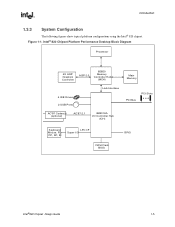
Figure 1-1. Introduction 1.3.3 System Configuration The following figures show typical platform configurations using the Intel® 820 chipset. Intel® 820 Chipset Platform Performance Desktop Block Diagram Processor 4X AGP Graphics Controller AGP 2.0 82820 Memory Controller Hub (MCH) Main Memory 4 IDE Drives 2 USB Ports Hub Interface PCI Bus PCI Slots AC'97 Codec(s) (optional) AC'97 2.1 82801AA I/O Controller Hub (ICH) Keyboard, Mouse, FD, PP, SP, IR LPC I/F Super I/O FWH Flash BIOS GPIO Intel®820 Chipset Design Guide 1-5
Figure 1-1. Introduction 1.3.3 System Configuration The following figures show typical platform configurations using the Intel® 820 chipset. Intel® 820 Chipset Platform Performance Desktop Block Diagram Processor 4X AGP Graphics Controller AGP 2.0 82820 Memory Controller Hub (MCH) Main Memory 4 IDE Drives 2 USB Ports Hub Interface PCI Bus PCI Slots AC'97 Codec(s) (optional) AC'97 2.1 82801AA I/O Controller Hub (ICH) Keyboard, Mouse, FD, PP, SP, IR LPC I/F Super I/O FWH Flash BIOS GPIO Intel®820 Chipset Design Guide 1-5

Design Guide
Page 20
... multiple data) Extensions. The Pentium III processor new extensions complement the Intel MMX™ technology SIMD extensions and provide a performance boost to RDRAM's performance features, the new memory architecture provides enhanced power management capabilities. Hub Interface As I/O speeds increase... operation; twice the AGP bandwidth of operation enables Intel® 820 chipset based systems to cost-effectively support suspend-to impact PCI bus performance. In conjunction with Direct Rambus* memory technology, allows graphics controllers to obtain optimal performance ...
... multiple data) Extensions. The Pentium III processor new extensions complement the Intel MMX™ technology SIMD extensions and provide a performance boost to RDRAM's performance features, the new memory architecture provides enhanced power management capabilities. Hub Interface As I/O speeds increase... operation; twice the AGP bandwidth of operation enables Intel® 820 chipset based systems to cost-effectively support suspend-to impact PCI bus performance. In conjunction with Direct Rambus* memory technology, allows graphics controllers to obtain optimal performance ...

Design Guide
Page 21
...detecting an ECC error, the MCH can decode this alert message and send a message over ALERTCLK and ALERTDATA. Also, no longer decode I/O, memory, or PCI configuration space. The ICH can use to recover from the disabled functions. Alert on LAN* The ICH supports Alert on RIMMs and..., CPU not booting) the ICH sends a message over the network to alert the network manager. SMBus The ICH integrates an SMBus controller. Intel®820 Chipset Design Guide 1-9 This timer is activated by the system case being opened. Once disabled, these functions no interrupts or power ...
...detecting an ECC error, the MCH can decode this alert message and send a message over ALERTCLK and ALERTDATA. Also, no longer decode I/O, memory, or PCI configuration space. The ICH can use to recover from the disabled functions. Alert on LAN* The ICH supports Alert on RIMMs and..., CPU not booting) the ICH sends a message over the network to alert the network manager. SMBus The ICH integrates an SMBus controller. Intel®820 Chipset Design Guide 1-9 This timer is activated by the system case being opened. Once disabled, these functions no interrupts or power ...

Design Guide
Page 48
...via and a real via. The high-speed CMOS signals must be matched in ) due to a timing requirement between RIMMs. Refer to the Intel® 820 Chipset: Intel® 82820 Memory Controller Hub (MCH) Datasheet for each clock, the following section for more information on Via Compensation. 2-22...must be used: Equation 2-3. To calculate the length for component package dimensions. RDRAM Trace Length Matching Example L1, L2 -> Package Dimensions L3, L4 -> Board Trace Length L1 MCH Package MCH Die Ball L3 L2 L4 L1 + L3 = Nominal RSL Length ±10 mils L2 + L4 = Nominal RSL Length...
...via and a real via. The high-speed CMOS signals must be matched in ) due to a timing requirement between RIMMs. Refer to the Intel® 820 Chipset: Intel® 82820 Memory Controller Hub (MCH) Datasheet for each clock, the following section for more information on Via Compensation. 2-22...must be used: Equation 2-3. To calculate the length for component package dimensions. RDRAM Trace Length Matching Example L1, L2 -> Package Dimensions L3, L4 -> Board Trace Length L1 MCH Package MCH Die Ball L3 L2 L4 L1 + L3 = Nominal RSL Length ±10 mils L2 + L4 = Nominal RSL Length...

Design Guide
Page 56
...• Clean VREF Routing - The traces must be ground isolated with no ground isolation) when they must have an additional trace length of the motherboard. - Clock signals must be ENTIRELY referenced to the MCH (and the 1st RIMM) as a differential pair. Clock signals must be on page ... length matched within ±10 mils of ) power plane splits. Signals must be possible to route as shown in the Intel® 820 chipset: 82820 Memory Controller Hub (MCH) Datasheet to the termination. For very short sections under the MCH and under these sections, the clocks ...
...• Clean VREF Routing - The traces must be ground isolated with no ground isolation) when they must have an additional trace length of the motherboard. - Clock signals must be ENTIRELY referenced to the MCH (and the 1st RIMM) as a differential pair. Clock signals must be on page ... length matched within ±10 mils of ) power plane splits. Signals must be possible to route as shown in the Intel® 820 chipset: 82820 Memory Controller Hub (MCH) Datasheet to the termination. For very short sections under the MCH and under these sections, the clocks ...

Design Guide
Page 111
...document addresses AGTL+ layout for both 1 and 2-way 133 MHz/100 MHz processor/ Intel® 820 chipset systems. Power distribution and chassis requirements for cooling, connector location, memory location, etc., may be sure to validate signal quality after making any changes in ...a different group. Always be obtained by more attention during the layout and validation portions of this technique. therefore, constraining the board routing. Advanced System Bus Design interference from this negative voltage can sum to change the network's noise margin, but mechanical constraints...
...document addresses AGTL+ layout for both 1 and 2-way 133 MHz/100 MHz processor/ Intel® 820 chipset systems. Power distribution and chassis requirements for cooling, connector location, memory location, etc., may be sure to validate signal quality after making any changes in ...a different group. Always be obtained by more attention during the layout and validation portions of this technique. therefore, constraining the board routing. Advanced System Bus Design interference from this negative voltage can sum to change the network's noise margin, but mechanical constraints...

Design Guide
Page 140
...DRCG Ratio. DRCG Ratio Mult[0:1] 0:0 0:1 1:0 1:1 DRCG 4:1 6:1 8:3 8:1 DRCG+ 9:2 6:1 16:3 8:1 4-12 Intel®820 Chipset Design Guide The device has the same specifications, pinout and form-factor as the existing DRCG device document. An... Termination to VSS 30 Ohms 40 Ohms 33 Ohms 4.7 Decoupling Recommendation for 300 MHz and 400 MHz memory bus is unchanged. However, pads should be tied to ground through a series resistor approximately the impedance ...and Jitter Specification To allow additional flexibility in board design, Intel has enabled a variation of the DRCG labeled the DRCG+.
...DRCG Ratio. DRCG Ratio Mult[0:1] 0:0 0:1 1:0 1:1 DRCG 4:1 6:1 8:3 8:1 DRCG+ 9:2 6:1 16:3 8:1 4-12 Intel®820 Chipset Design Guide The device has the same specifications, pinout and form-factor as the existing DRCG device document. An... Termination to VSS 30 Ohms 40 Ohms 33 Ohms 4.7 Decoupling Recommendation for 300 MHz and 400 MHz memory bus is unchanged. However, pads should be tied to ground through a series resistor approximately the impedance ...and Jitter Specification To allow additional flexibility in board design, Intel has enabled a variation of the DRCG labeled the DRCG+.
Design Guide
Page 145
...Flash BIOS). The 12V Vpp would be accepted by a positive decode agent out on the motherboard. The VPP pin MUST be two devices positively decoding the same cycle. This change in ...cells. The FWH Flash BIOS supports Vpp of the signaling environment used for subtractive decode, these memory cycles. If a PCI boot card is inserted and the ICH is critical to keep the ...is necessary to boot from a ROM behind the 82380AB. Stackup Requirement Overview The Intel® 820 chipset platform requires a board stackup with the 82380AB (ISA bridge), it is also necessary to attain the ...
...Flash BIOS). The 12V Vpp would be accepted by a positive decode agent out on the motherboard. The VPP pin MUST be two devices positively decoding the same cycle. This change in ...cells. The FWH Flash BIOS supports Vpp of the signaling environment used for subtractive decode, these memory cycles. If a PCI boot card is inserted and the ICH is critical to keep the ...is necessary to boot from a ROM behind the 82380AB. Stackup Requirement Overview The Intel® 820 chipset platform requires a board stackup with the 82380AB (ISA bridge), it is also necessary to attain the ...
Design Guide
Page 147
... 5-1 and following as a starting point: W=13.5 mil, H1=7 mil, H2=5, T=1.2 With these parameters, initial TDR should be used to ensure boards are possible, it is recommended to use the following figures: Table 5-1. 28Ω Stackup Examples Sample Zo H W T SM(max) Resin % ...2nd Choice = • 3rd Choice = Memory section of the motherboard Any section of the motherboard Separate location in the panel The Intel Impedance Test Methodology Document should be used . Incorporating a test coupon design into the motherboard makes testing simpler and more accurate. System ...
... 5-1 and following as a starting point: W=13.5 mil, H1=7 mil, H2=5, T=1.2 With these parameters, initial TDR should be used to ensure boards are possible, it is recommended to use the following figures: Table 5-1. 28Ω Stackup Examples Sample Zo H W T SM(max) Resin % ...2nd Choice = • 3rd Choice = Memory section of the motherboard Any section of the motherboard Separate location in the panel The Intel Impedance Test Methodology Document should be used . Incorporating a test coupon design into the motherboard makes testing simpler and more accurate. System ...
Design Guide
Page 153
...(S3) and Soft-off . This state is used in main memory and all unnecessary system logic is turned off (S5). Suspend operation During suspend operation, power is removed from some components on the Intel® 820 Chipset Reference Board. Power rails An ATX power supply has 6 power rails: +...are other power rails are on at different times (depending on the Intel® 820 Chipset Reference Board, 3.3VSB is derived from 5VSB using an on-board voltage regulator. For example, 3.3VSB is usually derived (on the motherboard) from 5V_DUAL). Dual power rail A dual power rail is derived ...
...(S3) and Soft-off . This state is used in main memory and all unnecessary system logic is turned off (S5). Suspend operation During suspend operation, power is removed from some components on the Intel® 820 Chipset Reference Board. Power rails An ATX power supply has 6 power rails: +...are other power rails are on at different times (depending on the Intel® 820 Chipset Reference Board, 3.3VSB is derived from 5VSB using an on-board voltage regulator. For example, 3.3VSB is usually derived (on the motherboard) from 5V_DUAL). Dual power rail A dual power rail is derived ...

Design Guide
Page 154
...the requirements of the change. 6-2 Intel®820 Chipset Design Guide It is critical, when deviating from these examples in any given time (i.e., only one of the devices may be driving the bus at any way, to consider the effect of main memory and PCI 3.3V aux (and ...VDDQ 3.3V VTT 3.3VSB 12V 2.5VSBY 2.5V The examples given in this Design Guide are only examples. power is accounted for the Intel® 820 Chipset Reference Board. This power delivery architecture supports the "Instantly Available PC Design Guidelines" via 3.3V aux) and USB (USB can only be completed....
...the requirements of the change. 6-2 Intel®820 Chipset Design Guide It is critical, when deviating from these examples in any given time (i.e., only one of the devices may be driving the bus at any way, to consider the effect of main memory and PCI 3.3V aux (and ...VDDQ 3.3V VTT 3.3VSB 12V 2.5VSBY 2.5V The examples given in this Design Guide are only examples. power is accounted for the Intel® 820 Chipset Reference Board. This power delivery architecture supports the "Instantly Available PC Design Guidelines" via 3.3V aux) and USB (USB can only be completed....
Design Guide
Page 157
... 6.1.3.2, "Option 2: Increase the Current Capability of the 2.5V Voltage Regulator" on the voltage sequencing requirements, refer to the latest Intel® 820 Chipset: 82820 Memory Controller Hub (MCH) datasheet. 3.3VSB The 3.3VSB plane powers the suspend well of excessive current will result in S3 (because... the ICH core is required in Figure 6-1. Note: This regulator is 7.5A, in a Intel® 820 chipset based system that ...
... 6.1.3.2, "Option 2: Increase the Current Capability of the 2.5V Voltage Regulator" on the voltage sequencing requirements, refer to the latest Intel® 820 Chipset: 82820 Memory Controller Hub (MCH) datasheet. 3.3VSB The 3.3VSB plane powers the suspend well of excessive current will result in S3 (because... the ICH core is required in Figure 6-1. Note: This regulator is 7.5A, in a Intel® 820 chipset based system that ...
Design Guide
Page 163
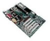
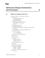
...Processor A A.1 Reference Design Feature Set The reference schematics feature the following core feature set: • Intel® 820 Chipset - Memory Controller Hub (MCH) - Debug Port • IOAPIC Integrated into the ICH • Direct RDRAM Memory Interface - 266 MHz, 300 MHz, 356 MHz and 400 MHz Direct RDRAM Support • 4 ... Interface • Support for the Pentium III (SC242) Processor - 100/133 MHz System Bus Frequency - APM Rev. 1.2 Compliant • Pentium III on-board VRM 8.4 compliant regulator • 4 Layer Design Intel®820 Chipset Design Guide A-1 I /O -
...Processor A A.1 Reference Design Feature Set The reference schematics feature the following core feature set: • Intel® 820 Chipset - Memory Controller Hub (MCH) - Debug Port • IOAPIC Integrated into the ICH • Direct RDRAM Memory Interface - 266 MHz, 300 MHz, 356 MHz and 400 MHz Direct RDRAM Support • 4 ... Interface • Support for the Pentium III (SC242) Processor - 100/133 MHz System Bus Frequency - APM Rev. 1.2 Compliant • Pentium III on-board VRM 8.4 compliant regulator • 4 Layer Design Intel®820 Chipset Design Guide A-1 I /O -

Design Guide
Page 170
... C 3 PWROK_CTRL B 1 2 MMBT3904LT1 E LCMD 11 R346 LSIO SBA0 SBA1 SBA2 SBA3 SBA4 SBA5 SBA6 SBA7 3 MMBT3904LT1 SBA[7:0] 11 19 Q9 C 3 B1 2 E A TITLE: INTEL(R) 820 CHIPSET CUSTOMER REFERENCE BOARD MCH R PCD PLATFORM DESIGN DRAWN BY: 1900 PRAIRIE CITY ROAD FOLSOM, CALIFORNIA 95630 LAST REVISED: 11-18-1999_11:34 2 1 REV: 1.01 PROJECT: SHEET... W15 ST0 Y15 ST1 Y17 ST2 J19 AD_STB0 H20 AD_STB#0 R18 AD_STB1 R19 AD_STB#1 Y20 SB_STB Y19 SB_STB# AGP 7 6 5 4 3 2 1 HUB MEMORY AGP HL0 F19 HL1 F18 HL2 E17 HL3 E19 HL4 B20 HL5 B19 HL6 B18 HL7 A20 HL8 D17 HL9 C18 HL10 D18 HL_STB D19...
... C 3 PWROK_CTRL B 1 2 MMBT3904LT1 E LCMD 11 R346 LSIO SBA0 SBA1 SBA2 SBA3 SBA4 SBA5 SBA6 SBA7 3 MMBT3904LT1 SBA[7:0] 11 19 Q9 C 3 B1 2 E A TITLE: INTEL(R) 820 CHIPSET CUSTOMER REFERENCE BOARD MCH R PCD PLATFORM DESIGN DRAWN BY: 1900 PRAIRIE CITY ROAD FOLSOM, CALIFORNIA 95630 LAST REVISED: 11-18-1999_11:34 2 1 REV: 1.01 PROJECT: SHEET... W15 ST0 Y15 ST1 Y17 ST2 J19 AD_STB0 H20 AD_STB#0 R18 AD_STB1 R19 AD_STB#1 Y20 SB_STB Y19 SB_STB# AGP 7 6 5 4 3 2 1 HUB MEMORY AGP HL0 F19 HL1 F18 HL2 E17 HL3 E19 HL4 B20 HL5 B19 HL6 B18 HL7 A20 HL8 D17 HL9 C18 HL10 D18 HL_STB D19...

Design Guide
Page 181
...10UF 16V 0.1UF R316 4.7K R252 1M R359 100K SW1 IDE_ACTIVE AC97_SPKR 13 PC_BEEP ICH has internal pullup and debounce on to prevent hot swapping memory. C322 14 0.1UF R326 4.7K VCC3_3SBY VCC3_3SBY VCC3_3SBY VCC3_3SBY JP23 1 2 3 U14 VCC 9 GPIO23_FPLED 3 4 GND SN74LVC07A LED_PU0 1 2... U14 65 PWM2 12 PWM outputs from SIO need power buffers for driving fan inputs. GPIO26_FPLED 9 GND SN74LVC07A A TITLE: INTEL(R) 820 CHIPSET CUSTOMER REFERENCE BOARD REV: SYSTEM 1.01 R PCD PLATFORM DESIGN DRAWN BY: PROJECT: 1900 PRAIRIE CITY ROAD FOLSOM, CALIFORNIA 95630 LAST REVISED: SHEET...
...10UF 16V 0.1UF R316 4.7K R252 1M R359 100K SW1 IDE_ACTIVE AC97_SPKR 13 PC_BEEP ICH has internal pullup and debounce on to prevent hot swapping memory. C322 14 0.1UF R326 4.7K VCC3_3SBY VCC3_3SBY VCC3_3SBY VCC3_3SBY JP23 1 2 3 U14 VCC 9 GPIO23_FPLED 3 4 GND SN74LVC07A LED_PU0 1 2... U14 65 PWM2 12 PWM outputs from SIO need power buffers for driving fan inputs. GPIO26_FPLED 9 GND SN74LVC07A A TITLE: INTEL(R) 820 CHIPSET CUSTOMER REFERENCE BOARD REV: SYSTEM 1.01 R PCD PLATFORM DESIGN DRAWN BY: PROJECT: 1900 PRAIRIE CITY ROAD FOLSOM, CALIFORNIA 95630 LAST REVISED: SHEET...
Design Guide
Page 203
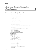
...Connector and Audio Codec • WfM Support • Integrated System Management • Integrated Power Management - ACPI Rev. 1.0 Compliant - Memory Controller Hub (MCH) - FWH Flash BIOS interface • Support for the two Pentium III (SC242) Processors - 100/133 MHz ...Connector • LPC Ultra I /O Controller Hub (ICH) - APM Rev. 1.2 Compliant • Pentium III on-board VRM 8.4 compliant regulator • 4 Layer Design Intel®820 Chipset Design Guide B-1 Reference Design Schematics: Dual-Processor Reference Design Schematics: Dual-Processor B B.1 Reference Design...
...Connector and Audio Codec • WfM Support • Integrated System Management • Integrated Power Management - ACPI Rev. 1.0 Compliant - Memory Controller Hub (MCH) - FWH Flash BIOS interface • Support for the two Pentium III (SC242) Processors - 100/133 MHz ...Connector • LPC Ultra I /O Controller Hub (ICH) - APM Rev. 1.2 Compliant • Pentium III on-board VRM 8.4 compliant regulator • 4 Layer Design Intel®820 Chipset Design Guide B-1 Reference Design Schematics: Dual-Processor Reference Design Schematics: Dual-Processor B B.1 Reference Design...

Design Guide
Page 212
...PWROK_CTRL B 1 2 MMBT3904LT1 E LCMD 13 R346 LSIO SBA0 SBA1 SBA2 SBA3 SBA4 SBA5 SBA6 SBA7 3 MMBT3904LT1 SBA[7:0] 13 21 Q9 C 3 B1 2 E A TITLE: INTEL(R) 820 CHIPSET DUAL PROCESSOR CUSTOMER REFERENCE BOARD REV: MCH 3.03 R PCD PLATFORM DESIGN DRAWN BY: PROJECT: 1900 PRAIRIE CITY ROAD FOLSOM, CALIFORNIA 95630 LAST REVISED: SHEET: 11-29-1999_14...W15 ST0 Y15 ST1 Y17 ST2 J19 AD_STB0 H20 AD_STB#0 R18 AD_STB1 R19 AD_STB#1 Y20 SB_STB Y19 SB_STB# AGP 7 6 5 4 3 2 1 HUB MEMORY AGP HL0 F19 HL1 F18 HL2 E17 HL3 E19 HL4 B20 HL5 B19 HL6 B18 HL7 A20 HL8 D17 HL9 C18 HL10 D18 HL_STB D19...
...PWROK_CTRL B 1 2 MMBT3904LT1 E LCMD 13 R346 LSIO SBA0 SBA1 SBA2 SBA3 SBA4 SBA5 SBA6 SBA7 3 MMBT3904LT1 SBA[7:0] 13 21 Q9 C 3 B1 2 E A TITLE: INTEL(R) 820 CHIPSET DUAL PROCESSOR CUSTOMER REFERENCE BOARD REV: MCH 3.03 R PCD PLATFORM DESIGN DRAWN BY: PROJECT: 1900 PRAIRIE CITY ROAD FOLSOM, CALIFORNIA 95630 LAST REVISED: SHEET: 11-29-1999_14...W15 ST0 Y15 ST1 Y17 ST2 J19 AD_STB0 H20 AD_STB#0 R18 AD_STB1 R19 AD_STB#1 Y20 SB_STB Y19 SB_STB# AGP 7 6 5 4 3 2 1 HUB MEMORY AGP HL0 F19 HL1 F18 HL2 E17 HL3 E19 HL4 B20 HL5 B19 HL6 B18 HL7 A20 HL8 D17 HL9 C18 HL10 D18 HL_STB D19...


