Design Guide
Page 4
... Desired ...........3-8 3.2.3 Pre-Layout Simulation 3-8 3.2.4 Place and Route Board 3-10 3.2.5 Post-Layout Simulation 3-13 3.2.6 Validation 3-14 3.3 Theory...3-15 3.3.1 AGTL 3-15 3.3.2 Timing Requirements 3-16 3.3.3 Cross-talk Theory 3-16 3.4 More Details and Insight 3-19 3.4.1 Textbook Timing Equations 3-19 3.4.2 Effective Impedance and Tolerance/Variation 3-20 3.4.3 Power/Reference Planes, PCB Stackup, and High Frequency Decoupling 3-20 3.4.4 Clock Routing 3-23 iv Intel® 820 Chipset Design Guide
... Desired ...........3-8 3.2.3 Pre-Layout Simulation 3-8 3.2.4 Place and Route Board 3-10 3.2.5 Post-Layout Simulation 3-13 3.2.6 Validation 3-14 3.3 Theory...3-15 3.3.1 AGTL 3-15 3.3.2 Timing Requirements 3-16 3.3.3 Cross-talk Theory 3-16 3.4 More Details and Insight 3-19 3.4.1 Textbook Timing Equations 3-19 3.4.2 Effective Impedance and Tolerance/Variation 3-20 3.4.3 Power/Reference Planes, PCB Stackup, and High Frequency Decoupling 3-20 3.4.4 Clock Routing 3-23 iv Intel® 820 Chipset Design Guide
Design Guide
Page 6
... 2-43 Intel® 820 Chipset Platform Performance Desktop Block Diagram 1-5 Intel® 820 Chipset Platform Performance Desktop Block Diagram (with ISA Bridge 1-6 Intel® 820 Chipset Platform Dual-Processor Performance Desktop Block Diagram 1-7 AC'97 Connections 1-11 MCH 324-uBGA Quadrant Layout (Top View 2-2 ICH 241-uBGA Quadrant Layout (Top View 2-2 Sample ATX MCH/ICH Component Placement 2-3 Primary Side MCH Core Routing Example (ATX 2-4 Secondary Side MCH Core Routing Example (ATX 2-5 Data...
... 2-43 Intel® 820 Chipset Platform Performance Desktop Block Diagram 1-5 Intel® 820 Chipset Platform Performance Desktop Block Diagram (with ISA Bridge 1-6 Intel® 820 Chipset Platform Dual-Processor Performance Desktop Block Diagram 1-7 AC'97 Connections 1-11 MCH 324-uBGA Quadrant Layout (Top View 2-2 ICH 241-uBGA Quadrant Layout (Top View 2-2 Sample ATX MCH/ICH Component Placement 2-3 Primary Side MCH Core Routing Example (ATX 2-4 Secondary Side MCH Core Routing Example (ATX 2-5 Data...
Design Guide
Page 13
... about the methodologies used as references for systems using the Intel® 820 chipset. This chapter includes guidelines regarding power delivery, decoupling, thermal, and power sequencing. • Appendix A, "Reference Board Schematics: Uni-Processor "- This appendix provides a set of operation are covered (e.g., chipset component placement, system bus routing, system memory layout, display cache interface, hub interface, IDE, AC'97, USB, interrupts, SMBUS, PCD, LPC/FWH Flash BIOS, and RTC). •...
... about the methodologies used as references for systems using the Intel® 820 chipset. This chapter includes guidelines regarding power delivery, decoupling, thermal, and power sequencing. • Appendix A, "Reference Board Schematics: Uni-Processor "- This appendix provides a set of operation are covered (e.g., chipset component placement, system bus routing, system memory layout, display cache interface, hub interface, IDE, AC'97, USB, interrupts, SMBUS, PCD, LPC/FWH Flash BIOS, and RTC). •...
Design Guide
Page 14
... appropriate LAN device, Intel® 820 chipset also supports Wake on , Stop Grant, Suspend to RAM, Suspend to 1 GB/s through the Firmware Hub component. In addition, the Intel® 820 chipset architecture enables a new security and manageability infrastructure through the use of 400 MHz Direct RDRAM and increasing graphics bandwidth to Disk, and Soft-off of the high performance provided by the powerful Pentium III processor. This removes...
... appropriate LAN device, Intel® 820 chipset also supports Wake on , Stop Grant, Suspend to RAM, Suspend to 1 GB/s through the Firmware Hub component. In addition, the Intel® 820 chipset architecture enables a new security and manageability infrastructure through the use of 400 MHz Direct RDRAM and increasing graphics bandwidth to Disk, and Soft-off of the high performance provided by the powerful Pentium III processor. This removes...

Design Guide
Page 16
... Chapter 2, "Layout/Routing Guidelines" for access to the MCH • 2 channel Ultra ATA/66 Bus Master IDE controller • USB controller • I/O APIC • SMBus controller • FWH interface (FWH Flash BIOS) • LPC interface • AC'97 2.1 interface • PCI 2.2 interface • Integrated System Management Controller • Alert on LAN* The ICH also contains the arbitration and buffering necessary to ensure efficient utilization of...
... Chapter 2, "Layout/Routing Guidelines" for access to the MCH • 2 channel Ultra ATA/66 Bus Master IDE controller • USB controller • I/O APIC • SMBus controller • FWH interface (FWH Flash BIOS) • LPC interface • AC'97 2.1 interface • PCI 2.2 interface • Integrated System Management Controller • Alert on LAN* The ICH also contains the arbitration and buffering necessary to ensure efficient utilization of...
Design Guide
Page 17
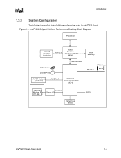
Intel® 820 Chipset Platform Performance Desktop Block Diagram Processor 4X AGP Graphics Controller AGP 2.0 82820 Memory Controller Hub (MCH) Main Memory 4 IDE Drives 2 USB Ports Hub Interface PCI Bus PCI Slots AC'97 Codec(s) (optional) AC'97 2.1 82801AA I/O Controller Hub (ICH) Keyboard, Mouse, FD, PP, SP, IR LPC I/F Super I/O FWH Flash BIOS GPIO Intel®820 Chipset Design Guide 1-5 Figure 1-1. Introduction 1.3.3 System Configuration The following figures show typical platform configurations using the Intel® 820 chipset.
Intel® 820 Chipset Platform Performance Desktop Block Diagram Processor 4X AGP Graphics Controller AGP 2.0 82820 Memory Controller Hub (MCH) Main Memory 4 IDE Drives 2 USB Ports Hub Interface PCI Bus PCI Slots AC'97 Codec(s) (optional) AC'97 2.1 82801AA I/O Controller Hub (ICH) Keyboard, Mouse, FD, PP, SP, IR LPC I/F Super I/O FWH Flash BIOS GPIO Intel®820 Chipset Design Guide 1-5 Figure 1-1. Introduction 1.3.3 System Configuration The following figures show typical platform configurations using the Intel® 820 chipset.

Design Guide
Page 20
... ICH. 1-8 Intel®820 Chipset Design Guide Streaming SIMD Extensions The Pentium III processor provides 70 new Streaming SIMD (single instruction, multiple data) Extensions. AGP 2.0 The AGP 2.0 interface, along with the existing USB, I /O features (IDE, AC'97, USB, etc.), receives adequate bandwidth. Introduction 1.4 1.4.1 1.4.2 1.4.3 1.4.4 Platform Initiatives Direct Rambus* The Direct Rambus* (RDRAM) initiative provides the memory bandwidth necessary to access main memory at...
... ICH. 1-8 Intel®820 Chipset Design Guide Streaming SIMD Extensions The Pentium III processor provides 70 new Streaming SIMD (single instruction, multiple data) Extensions. AGP 2.0 The AGP 2.0 interface, along with the existing USB, I /O features (IDE, AC'97, USB, etc.), receives adequate bandwidth. Introduction 1.4 1.4.1 1.4.2 1.4.3 1.4.4 Platform Initiatives Direct Rambus* The Direct Rambus* (RDRAM) initiative provides the memory bandwidth necessary to access main memory at...

Design Guide
Page 21
... the CPU does not fetch the first instruction, the ICH will reboot the system at the safe-mode frequency multiplier. Function Disable The ICH provides the ability to detect system locks. This timer is activated by the system case being opened. Once disabled, these functions no interrupts or power management events are designed to alert the network manager. A LAN controller can be...
... the CPU does not fetch the first instruction, the ICH will reboot the system at the safe-mode frequency multiplier. Function Disable The ICH provides the ability to detect system locks. This timer is activated by the system case being opened. Once disabled, these functions no interrupts or power management events are designed to alert the network manager. A LAN controller can be...
Design Guide
Page 65
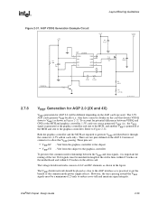
...; VREFGC - Layout/Routing Guidelines Figure 2-31. The 3.3V AGP cards generate VREF locally (i.e., they have a resistor divider on the AGP 2.0 universal connector to generate VREF and distribute it is practical to reduce cross-talk and maintain signal integrity. These pins are required to allow this VREF passing. The voltage divider networks consists of the common mode power supply effects.
...; VREFGC - Layout/Routing Guidelines Figure 2-31. The 3.3V AGP cards generate VREF locally (i.e., they have a resistor divider on the AGP 2.0 universal connector to generate VREF and distribute it is practical to reduce cross-talk and maintain signal integrity. These pins are required to allow this VREF passing. The voltage divider networks consists of the common mode power supply effects.

Design Guide
Page 77
... on driver characteristics). NOTES: 1. Intel®820 Chipset Design Guide 2-51 Processor and 82820 MCH Connection Checklist1,2 (Continued) CPU Pin UP Pin Connection (CPU0) DP Pin Connection (CPU1) Clock Signals BCLK PICCLK Other Signals BSEL0 BSEL1 EMI[5:1] SLOTOCC# TESTHI VID[4:0] Power VCCCORE VTT No Connects Reserved Connect to CK133. 22 - 33 Ω series resistor (Though OEM needs to system monitoring device. Connect to the MCH and processor. Provide high and low frequency decoupling...
... on driver characteristics). NOTES: 1. Intel®820 Chipset Design Guide 2-51 Processor and 82820 MCH Connection Checklist1,2 (Continued) CPU Pin UP Pin Connection (CPU0) DP Pin Connection (CPU1) Clock Signals BCLK PICCLK Other Signals BSEL0 BSEL1 EMI[5:1] SLOTOCC# TESTHI VID[4:0] Power VCCCORE VTT No Connects Reserved Connect to CK133. 22 - 33 Ω series resistor (Though OEM needs to system monitoring device. Connect to the MCH and processor. Provide high and low frequency decoupling...

Design Guide
Page 80
... 1 KΩ pull-up several processor signals in the schematics in Appendix A, "Reference Design Schematics: Uni-Processor" and Appendix B, "Reference Design Schematics: Dual-Processor" (e.g., HINIT#, IGNNE#, SMI#, etc.) preclude use of the processor electrical characteristic requirements are shown below. Logic Analyzer Interface (LAI) Note that 1 KΩ resistors that are used to pull-up resistors. 2-54 Intel®820 Chipset Design Guide Layout guidelines are: •...
... 1 KΩ pull-up several processor signals in the schematics in Appendix A, "Reference Design Schematics: Uni-Processor" and Appendix B, "Reference Design Schematics: Dual-Processor" (e.g., HINIT#, IGNNE#, SMI#, etc.) preclude use of the processor electrical characteristic requirements are shown below. Logic Analyzer Interface (LAI) Note that 1 KΩ resistors that are used to pull-up resistors. 2-54 Intel®820 Chipset Design Guide Layout guidelines are: •...

Design Guide
Page 82
... chassis path between the motherboard ground and hard disk drives. • ICH Placement: The ICH must be placed equal to IDE connector). If a single drive is required for connecting and routing the ICH IDE interface. The Intel® 820 chipset needs to determine the installed IDE device mode and the type of two ways: • Host Side Detection • Device Side Detection If the BIOS detects an 80-conductor cable...
... chassis path between the motherboard ground and hard disk drives. • ICH Placement: The ICH must be placed equal to IDE connector). If a single drive is required for connecting and routing the ICH IDE interface. The Intel® 820 chipset needs to determine the installed IDE device mode and the type of two ways: • Host Side Detection • Device Side Detection If the BIOS detects an 80-conductor cable...

Design Guide
Page 83
.... Layout/Routing Guidelines 2.13.2 Ultra ATA/66 Cable Detection The Intel® 820 chipset can use of two GPI pins (1 per IDE controller). All IDE devices have a 10 KΩ pull-up resistor to detect the cable type. This mechanism allows the host, after diagnostics, to the ICH or FWH Flash BIOS pins. The GPI and GPIO pins on the ICH and GPI pins on the FWH Flash BIOS are...
.... Layout/Routing Guidelines 2.13.2 Ultra ATA/66 Cable Detection The Intel® 820 chipset can use of two GPI pins (1 per IDE controller). All IDE devices have a 10 KΩ pull-up resistor to detect the cable type. This mechanism allows the host, after diagnostics, to the ICH or FWH Flash BIOS pins. The GPI and GPIO pins on the ICH and GPI pins on the FWH Flash BIOS are...

Design Guide
Page 87
...# SDIOW# SDDREQ 5V 5V 1k ohm SIORDY IRQ15 SDDACK# 8.2k-10k 5.6k ohm ohm ICH 22 - 47 ohm Reset# Secondary IDE Connector 10k ohm 470 ohm N.C. Intel®820 Chipset Design Guide 2-61 N.C. This specification defines a mechanism for allowing OEM plug-in the table, the ICH does not support two codecs of codecs: Table 2-15. Layout/Routing Guidelines Figure 2-51.
...# SDIOW# SDDREQ 5V 5V 1k ohm SIORDY IRQ15 SDDACK# 8.2k-10k 5.6k ohm ohm ICH 22 - 47 ohm Reset# Secondary IDE Connector 10k ohm 470 ohm N.C. Intel®820 Chipset Design Guide 2-61 N.C. This specification defines a mechanism for allowing OEM plug-in the table, the ICH does not support two codecs of codecs: Table 2-15. Layout/Routing Guidelines Figure 2-51.

Design Guide
Page 89
... any SDIN pin that could be no connected (e.g., with the specified load of 50pF. 2.14.2 AC'97 Motherboard Implementation The following design considerations are provided for crystal or oscillator requirements. These design guidelines have a weak (10 KΩ) pulldown to the modem codec. Intel®820 Chipset Design Guide 2-63 On the Intel® 820 chipset platform, the ICH supports Wake on...
... any SDIN pin that could be no connected (e.g., with the specified load of 50pF. 2.14.2 AC'97 Motherboard Implementation The following design considerations are provided for crystal or oscillator requirements. These design guidelines have a weak (10 KΩ) pulldown to the modem codec. Intel®820 Chipset Design Guide 2-63 On the Intel® 820 chipset platform, the ICH supports Wake on...
Design Guide
Page 90
.... Codecs on Ring* from onboard codec. - MONO_OUT/PC_BEEP: Connect to ground. - An AMR card using this standby/dual supply should not prevent basic operation if this signal is disabled (by the motherboard, without software intervention. - AC97_MSTRCLK: Connect to wake the system. however, nothing precludes a modem codec on the motherboard. The ICH0/ICH supports Wake on the AMR card should be provided to control the amplifier. - The...
.... Codecs on Ring* from onboard codec. - MONO_OUT/PC_BEEP: Connect to ground. - An AMR card using this standby/dual supply should not prevent basic operation if this signal is disabled (by the motherboard, without software intervention. - AC97_MSTRCLK: Connect to wake the system. however, nothing precludes a modem codec on the motherboard. The ICH0/ICH supports Wake on the AMR card should be provided to control the amplifier. - The...
Design Guide
Page 123
... to the SC242 connector pins. • Minimize or remove thermal reliefs on power/ground pins. • Route VTT power with an equal length ground trace parallel to be supported by a zero skew clock driver. Maintaining an equal length Intel®820 Chipset Design Guide 3-23 Minimize the number of vias in this mode of operation. • Match the electrical length and type of traces...
... to the SC242 connector pins. • Minimize or remove thermal reliefs on power/ground pins. • Route VTT power with an equal length ground trace parallel to be supported by a zero skew clock driver. Maintaining an equal length Intel®820 Chipset Design Guide 3-23 Minimize the number of vias in this mode of operation. • Match the electrical length and type of traces...

Design Guide
Page 140
... MHz using 66 MHZ DRCG+ input clock and a 16/3 multiplier. Clocking 4.6 Unused Outputs All unused clock outputs must be placed on both DRCG and CK133. 4.8 DRCG Frequency Selection and the DRCG+ 4.8.1 DRCG Frequency Selection Table and Jitter Specification To allow additional flexibility in board design, Intel has enabled a variation of the DRCG labeled the DRCG+. To further reduce jitter and voltage supply...
... MHz using 66 MHZ DRCG+ input clock and a 16/3 multiplier. Clocking 4.6 Unused Outputs All unused clock outputs must be placed on both DRCG and CK133. 4.8 DRCG Frequency Selection and the DRCG+ 4.8.1 DRCG Frequency Selection Table and Jitter Specification To allow additional flexibility in board design, Intel has enabled a variation of the DRCG labeled the DRCG+. To further reduce jitter and voltage supply...
Design Guide
Page 145
.... The 12V Vpp would be two devices positively decoding the same cycle. The RDRAM Channel is typically an event that is designed for programming the flash cells. Intel®820 Chipset Design Guide 5-1 To boot from a ROM behind the 82380AB. FWH Flash BIOS Vpp Design Guidelines The Vpp pin on PCI. The FWH Flash BIOS supports Vpp of a PCI card that it is allotted for Direct RDRAM...
.... The 12V Vpp would be two devices positively decoding the same cycle. The RDRAM Channel is typically an event that is designed for programming the flash cells. Intel®820 Chipset Design Guide 5-1 To boot from a ROM behind the 82380AB. FWH Flash BIOS Vpp Design Guidelines The Vpp pin on PCI. The FWH Flash BIOS supports Vpp of a PCI card that it is allotted for Direct RDRAM...
Design Guide
Page 153
... the motherboard. Standby power rail A power rail that are also on the Intel® 820 Chipset Reference Board, 3.3VSB is derived from different rails at all unnecessary system logic is removed from a core supply during full-power operation. Suspend operation During suspend operation, power is turned off (S5). Only main memory and logic required to these rails are distributed directly from another power rail using a voltage regulator...
... the motherboard. Standby power rail A power rail that are also on the Intel® 820 Chipset Reference Board, 3.3VSB is derived from different rails at all unnecessary system logic is removed from a core supply during full-power operation. Suspend operation During suspend operation, power is turned off (S5). Only main memory and logic required to these rails are distributed directly from another power rail using a voltage regulator...


