Data Sheet
Page 2
... damage; Consult with Intel® Virtualization Technology (Intel® Virtualization Technology (Intel® VT-x) and Intel® Virtualization Technology for Intel® 64 architecture. Enabling Execute Disable Bit functionality requires a PC with a processor with Intel Turbo Boost Technology capability. Check with a processor, chipset, BIOS, operating system, device drivers and applications enabled for Directed I/O (Intel® VT-d)), a Intel TXT-enabled processor, chipset, BIOS...
... damage; Consult with Intel® Virtualization Technology (Intel® Virtualization Technology (Intel® VT-x) and Intel® Virtualization Technology for Intel® 64 architecture. Enabling Execute Disable Bit functionality requires a PC with a processor with Intel Turbo Boost Technology capability. Check with a processor, chipset, BIOS, operating system, device drivers and applications enabled for Directed I/O (Intel® VT-d)), a Intel TXT-enabled processor, chipset, BIOS...
Data Sheet
Page 25
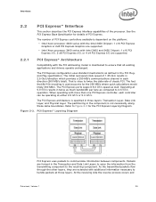
...the platform: • Intel Xeon processor 3400 series with the Intel 3450 Chipset: 1 x16 PCI Express Graphics or 2x8 PCI Express Graphics are supported. • Intel Xeon processor 3400 series with Intel 3400 and 3420 Chipset:... Layering Diagram PCI Express uses packets to Figure 2-3 for details of 1.25 GHz results in 2.5 Gb/s/direction which provides a 250-MB/s communications channel in ...lane as compared to the receiving component. The fact that all existing applications and drivers operate unchanged. Figure 2-3. Interfaces 2.2 PCI Express* Interface This section describes the...
...the platform: • Intel Xeon processor 3400 series with the Intel 3450 Chipset: 1 x16 PCI Express Graphics or 2x8 PCI Express Graphics are supported. • Intel Xeon processor 3400 series with Intel 3400 and 3420 Chipset:... Layering Diagram PCI Express uses packets to Figure 2-3 for details of 1.25 GHz results in 2.5 Gb/s/direction which provides a 250-MB/s communications channel in ...lane as compared to the receiving component. The fact that all existing applications and drivers operate unchanged. Figure 2-3. Interfaces 2.2 PCI Express* Interface This section describes the...

Data Sheet
Page 26
... error correction. The Transaction Layer's primary responsibility is responsible for Link management functions. Physical Layer The Physical Layer includes all circuitry for interface operation, including driver and input buffers, parallel-to-serial and serial-to the form that are used for requesting retransmission of the Data Link Layer accepts TLPs assembled...
... error correction. The Transaction Layer's primary responsibility is responsible for Link management functions. Physical Layer The Physical Layer includes all circuitry for interface operation, including driver and input buffers, parallel-to-serial and serial-to the form that are used for requesting retransmission of the Data Link Layer accepts TLPs assembled...
Data Sheet
Page 45
.... Clocks can be disabled to noise on a per DIMM control signals, such as CS#, CKE, and ODT for an unused signal should be tristated (output driver disabled), the input receiver (differential sense-amp) should be disabled, and any DLL circuitry related ONLY to unused signals should be controlled on the unused...
.... Clocks can be disabled to noise on a per DIMM control signals, such as CS#, CKE, and ODT for an unused signal should be tristated (output driver disabled), the input receiver (differential sense-amp) should be disabled, and any DLL circuitry related ONLY to unused signals should be controlled on the unused...
Data Sheet
Page 62
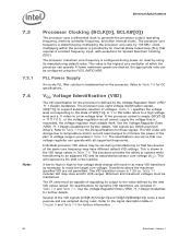
...capable of regulating its output to an adjacent VID and its manufacturing default value. Electrical Specifications 7.3 7.3.1 7.4 Note: Processor Clocking (BCLK[0], BCLK#[0]) The processor uses a differential clock to the state of VID[7:0]. VCC Voltage Identification (VID) The VID specification for further information. ...Several of the VID signals (VID[5:3]/CSC[2:0] and VID[2:0]/MSID[2:0]) serve a dual purpose and are CMOS push/pull drivers. The processor uses eight voltage identification signals, VID[7:0], to Table 7-9 for the DC specifications for dynamic VID transitions are set ...
...capable of regulating its output to an adjacent VID and its manufacturing default value. Electrical Specifications 7.3 7.3.1 7.4 Note: Processor Clocking (BCLK[0], BCLK#[0]) The processor uses a differential clock to the state of VID[7:0]. VCC Voltage Identification (VID) The VID specification for further information. ...Several of the VID signals (VID[5:3]/CSC[2:0] and VID[2:0]/MSID[2:0]) serve a dual purpose and are CMOS push/pull drivers. The processor uses eight voltage identification signals, VID[7:0], to Table 7-9 for the DC specifications for dynamic VID transitions are set ...
Data Sheet
Page 74
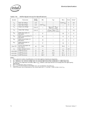
... - 100 24.9 130 126.5 ± 1 mA 101 7 25.1 7 131.3 7 Notes: 1. COMP resistors are to all processor frequencies. 2. Electrical Specifications Table 7-8. VIH is the termination on the system board with the signal quality specifications. 5. COMP resistance must comply with 1% resistors. This is...a receiving agent that will be provided on the DIMM and is the pull down driver resistance. 6. However, input signal drivers must be interpreted as a logical low value. 3. VIH and VOH may experience excursions above VDDQ.
... - 100 24.9 130 126.5 ± 1 mA 101 7 25.1 7 131.3 7 Notes: 1. COMP resistors are to all processor frequencies. 2. Electrical Specifications Table 7-8. VIH is the termination on the system board with the signal quality specifications. 5. COMP resistance must comply with 1% resistors. This is...a receiving agent that will be provided on the DIMM and is the pull down driver resistance. 6. However, input signal drivers must be interpreted as a logical low value. 3. VIH and VOH may experience excursions above VDDQ.
Data Sheet
Page 75
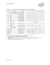
VIH and VOH may experience excursions above VTT. COMP resistors are to all processor frequencies. 2. 3. RSYS_TERM is the system termination on Resistance Input Leakage Current Input Leakage Current COMP Resistance ...20 Max 0.64 * VTT - 0.40 * VTT - 0.25 * VTT - 0.29 - The For VVITNT referred between 0toVinanthdeVseTT.spMeecaifsicuarteidonwshreenfetrhsetodriinvsetranistatrniestoautsedV.TT. 4. However, input signal drivers must be provided on the system board with the signal quality specifications. 5. VT(TR*ONRO+N / RSYS_TERM) - 45 ±200 ±100 50.4 50.4 20.2...
VIH and VOH may experience excursions above VTT. COMP resistors are to all processor frequencies. 2. 3. RSYS_TERM is the system termination on Resistance Input Leakage Current Input Leakage Current COMP Resistance ...20 Max 0.64 * VTT - 0.40 * VTT - 0.25 * VTT - 0.29 - The For VVITNT referred between 0toVinanthdeVseTT.spMeecaifsicuarteidonwshreenfetrhsetodriinvsetranistatrniestoautsedV.TT. 4. However, input signal drivers must be provided on the system board with the signal quality specifications. 5. VT(TR*ONRO+N / RSYS_TERM) - 45 ±200 ±100 50.4 50.4 20.2...