
Service Manual
Page 1
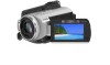
...233;cifié. DIGITAL VIDEO CAMERA RECORDER HDR-SR5/SR5C/SR5E/SR7/SR7E/SR8/SR8E_L2 9-852-202-32 Sony EMCS Co. 2007K0800-1 © 2007.11 Published by mark 0 or dotted line with mark 0 are critical for safety. HDR-SR5/SR5C/SR5E/SR7/SR7E/SR8/SR8E RMT.... Photo: HDR-SR5 2 LEVEL US Model Canadian Model AEP Model UK Model E Model Australian Model Hong Kong Model Chinese Model Korea Model Tourist Model Japanese Model Link SPECIFICATIONS DISASSEMBLY SCHEMATIC DIAGRAMS MODEL INFORMATION TABLE BLOCK DIAGRAMS PRINTED WIRING BOARDS SERVICE NOTE FRAME SCHEMATIC DIAGRAM REPAIR PARTS ...
...233;cifié. DIGITAL VIDEO CAMERA RECORDER HDR-SR5/SR5C/SR5E/SR7/SR7E/SR8/SR8E_L2 9-852-202-32 Sony EMCS Co. 2007K0800-1 © 2007.11 Published by mark 0 or dotted line with mark 0 are critical for safety. HDR-SR5/SR5C/SR5E/SR7/SR7E/SR8/SR8E RMT.... Photo: HDR-SR5 2 LEVEL US Model Canadian Model AEP Model UK Model E Model Australian Model Hong Kong Model Chinese Model Korea Model Tourist Model Japanese Model Link SPECIFICATIONS DISASSEMBLY SCHEMATIC DIAGRAMS MODEL INFORMATION TABLE BLOCK DIAGRAMS PRINTED WIRING BOARDS SERVICE NOTE FRAME SCHEMATIC DIAGRAM REPAIR PARTS ...
Service Manual
Page 6
... it is at a temperature about 350°C. HDR-SR5/SR5C/SR5E/SR7/SR7E/SR8/SR8E_L2 Unleaded solder Boards requiring use of unleaded solder are "pinched" or contact high-wattage resistors. 3. Soldering irons using a temperature ... replaced. NE REMPLACER CES COMPOSANTS QUE PAR DES PIÈSES SONY DONT LES NUMÉROS SONT DONNÉS DANS CE MANUEL OU DANS LES SUPPÉ...during a previous repair. COMPONENTS IDENTIFIED BY MARK 0 OR DOTTED LINE WITH MARK 0 ON THE SCHEMATIC DIAGRAMS AND IN THE PARTS LIST ARE CRITICAL TO SAFE OPERATION. Caution: The printed pattern (copper foil) ...
... it is at a temperature about 350°C. HDR-SR5/SR5C/SR5E/SR7/SR7E/SR8/SR8E_L2 Unleaded solder Boards requiring use of unleaded solder are "pinched" or contact high-wattage resistors. 3. Soldering irons using a temperature ... replaced. NE REMPLACER CES COMPOSANTS QUE PAR DES PIÈSES SONY DONT LES NUMÉROS SONT DONNÉS DANS CE MANUEL OU DANS LES SUPPÉ...during a previous repair. COMPONENTS IDENTIFIED BY MARK 0 OR DOTTED LINE WITH MARK 0 ON THE SCHEMATIC DIAGRAMS AND IN THE PARTS LIST ARE CRITICAL TO SAFE OPERATION. Caution: The printed pattern (copper foil) ...

Service Manual
Page 44
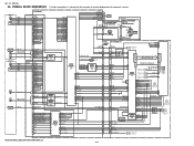
... (2/21) AD0_0 - BLOCK DIAGRAMS 3-1. AD3_13 D6 XSYS_RST H5 CLPOB K5 CHCK SR7/SR7E/SR8/SR8E 1 IC1701 FF 5 CHCK (4/21) X1701 80.919081MHz : SR5/SR5C 62.37MHz : SR5E 89.010989MHz : SR7/SR8 74.25MHz : SR7E/SR8E 08 : VIDEO SIGNAL HDR-SR5/SR5C/SR5E/SR7/SR7E/SR8/..., D3 E6, F6, G6 J4, K4, F5, G5 6M_DCOUT1, 2, 5, 6, 6M_DRVOUT1, 2, 5, 6 AD1_0 - OVERALL BLOCK DIAGRAM (1/7) ( ) : Number in parenthesis ( ) indicates the division number of schematic diagram where the component is located. AD0_13 AD2_0 - T23, U20, U21 B5, A5, C5, D5, E5 IC1301 TRIPLE CHANNEL ADC_2 (3/21...
... (2/21) AD0_0 - BLOCK DIAGRAMS 3-1. AD3_13 D6 XSYS_RST H5 CLPOB K5 CHCK SR7/SR7E/SR8/SR8E 1 IC1701 FF 5 CHCK (4/21) X1701 80.919081MHz : SR5/SR5C 62.37MHz : SR5E 89.010989MHz : SR7/SR8 74.25MHz : SR7E/SR8E 08 : VIDEO SIGNAL HDR-SR5/SR5C/SR5E/SR7/SR7E/SR8/..., D3 E6, F6, G6 J4, K4, F5, G5 6M_DCOUT1, 2, 5, 6, 6M_DRVOUT1, 2, 5, 6 AD1_0 - OVERALL BLOCK DIAGRAM (1/7) ( ) : Number in parenthesis ( ) indicates the division number of schematic diagram where the component is located. AD0_13 AD2_0 - T23, U20, U21 B5, A5, C5, D5, E5 IC1301 TRIPLE CHANNEL ADC_2 (3/21...

Service Manual
Page 45
..., C9, B9 STL_DATA/CCD_IN0-13, STL_DATA14-31 STL_ADDR0-11 STL_CLK, STL_CKE, STL_XCAS, STL_XWE, STL_XCS0, STL_XRAS A11 STL_BS0 D12 STL_BS1 B11 SD_DQM 08 HDR-SR5/SR5C/SR5E/SR7/SR7E/SR8/SR8E_L2 A9, D9, A10, B10, C10, A3 C12, B12, A12, D13, C13, B13, A13, A14,..., STL_XRAS SIGNAL AG15 PROCESS AG17 (4/21) STL_BS0 J15 AF16 STL_BS1 G14 AG10 Y25 Y26 EMC_DATA [0] - OVERALL BLOCK DIAGRAM (2/7) ( ) : Number in parenthesis ( ) indicates the division number of schematic diagram where the component is located. VIN_C7 EMC_XDQM[0-3] AE17, AH16, AD17, AH15 B19, D19, D18, A19, C18...
..., C9, B9 STL_DATA/CCD_IN0-13, STL_DATA14-31 STL_ADDR0-11 STL_CLK, STL_CKE, STL_XCAS, STL_XWE, STL_XCS0, STL_XRAS A11 STL_BS0 D12 STL_BS1 B11 SD_DQM 08 HDR-SR5/SR5C/SR5E/SR7/SR7E/SR8/SR8E_L2 A9, D9, A10, B10, C10, A3 C12, B12, A12, D13, C13, B13, A13, A14,..., STL_XRAS SIGNAL AG15 PROCESS AG17 (4/21) STL_BS0 J15 AF16 STL_BS1 G14 AG10 Y25 Y26 EMC_DATA [0] - OVERALL BLOCK DIAGRAM (2/7) ( ) : Number in parenthesis ( ) indicates the division number of schematic diagram where the component is located. VIN_C7 EMC_XDQM[0-3] AE17, AH16, AD17, AH15 B19, D19, D18, A19, C18...

Service Manual
Page 47
... ( ) indicates the division number of schematic diagram where the component is located. Ver. 1.1 2007...GSENS_REF BOOT_MODE_PORT0 H9 K7 GSENS_TEMP SR5E/SR7/SR7E/SR8/SR8E 13 3 1 SE3801 G SENSOR 4 5 J11 JACK_AD_CRADLE C5 XLANC_JACK_IN SR5/SR5C 10 5 SE3802 G SENSOR 9 8 13 OVERALL (5/7) (PAGE 3-5) 7 OVERALL (3/7) (PAGE 3-3) IC2901_Y_OUT 2 IC2901_C... PHOTO OFF (CHG) ON POWER MODE D002 (CHARGE/STROBE) *1 SR5/SR5C SR5E R1076 XX 0 R1077 0 XX SR7/SR8 100K 22K SR7E/SR8E 22K 100K 08 HDR-SR5/SR5C/SR5E/SR7/SR7E/SR8/SR8E_L2 3-4 XCAM_LED 15 XCAM_LED HDD_ACCESS 12 X_ACCESS_LED...
... ( ) indicates the division number of schematic diagram where the component is located. Ver. 1.1 2007...GSENS_REF BOOT_MODE_PORT0 H9 K7 GSENS_TEMP SR5E/SR7/SR7E/SR8/SR8E 13 3 1 SE3801 G SENSOR 4 5 J11 JACK_AD_CRADLE C5 XLANC_JACK_IN SR5/SR5C 10 5 SE3802 G SENSOR 9 8 13 OVERALL (5/7) (PAGE 3-5) 7 OVERALL (3/7) (PAGE 3-3) IC2901_Y_OUT 2 IC2901_C... PHOTO OFF (CHG) ON POWER MODE D002 (CHARGE/STROBE) *1 SR5/SR5C SR5E R1076 XX 0 R1077 0 XX SR7/SR8 100K 22K SR7E/SR8E 22K 100K 08 HDR-SR5/SR5C/SR5E/SR7/SR7E/SR8/SR8E_L2 3-4 XCAM_LED 15 XCAM_LED HDD_ACCESS 12 X_ACCESS_LED...

Service Manual
Page 48
...STRB_CHARGE 5 XSTRB_FULL 6 STROBE_ON 7 CN5202 10 SCHARGE_ON 9 XSCHARGE_FULL 8 STROBO_ON L5201 ST_UNREG 8 1 7 IC5201 4 2 FLASH CONTROL/ CHARGE CONTROL 6 08 HDR-SR5/SR5C/SR5E/SR7/SR7E/SR8/SR8E_L2 AP9 ADAPTOR_DET 3-5 ADAPTOR_DET 14 1 ADAPTER DETECT T5201 2 6 D5202 FLASH UNIT (FL25500) CN5201 XE_A 15 - 18... H32, H33 K33, J32 AM16, AN16 AN15, AN22 - Ver. 1.1 2007.06 3-5. OVERALL BLOCK DIAGRAM (5/7) ( ) : Number in parenthesis ( ) indicates the division number of schematic diagram where the component is located. HM_R7 Y12, AA12 HM_Y0 - HM_Y7 Y21, AA20 HM_B0 - A8, A9...
...STRB_CHARGE 5 XSTRB_FULL 6 STROBE_ON 7 CN5202 10 SCHARGE_ON 9 XSCHARGE_FULL 8 STROBO_ON L5201 ST_UNREG 8 1 7 IC5201 4 2 FLASH CONTROL/ CHARGE CONTROL 6 08 HDR-SR5/SR5C/SR5E/SR7/SR7E/SR8/SR8E_L2 AP9 ADAPTOR_DET 3-5 ADAPTOR_DET 14 1 ADAPTER DETECT T5201 2 6 D5202 FLASH UNIT (FL25500) CN5201 XE_A 15 - 18... H32, H33 K33, J32 AM16, AN16 AN15, AN22 - Ver. 1.1 2007.06 3-5. OVERALL BLOCK DIAGRAM (5/7) ( ) : Number in parenthesis ( ) indicates the division number of schematic diagram where the component is located. HM_R7 Y12, AA12 HM_Y0 - HM_Y7 Y21, AA20 HM_B0 - A8, A9...
Service Manual
Page 49
...(4/21) 3 OVERALL (2/7) (PAGE 3-2) 1 OVERALL (1/7) (PAGE 3-1) 46, 47 44, 45 42, 43 40, 41 08 HDR-SR5/SR5C/SR5E/SR7/SR7E/SR8/SR8E_L2 3-6 LENS BLOCK IRIS MOTOR M H LENS TEMP SENSOR ZOOM MOTOR M FOCUS MOTOR M LENS BLOCK..., ZOOM_XB, ZOOM_B FOCUS+, FOCUS- YAW- Ver. 1.1 2007.06 3-6. A9 ND_HALL- L7 NF_DRIVE+ L6 1 7 IC5401 FOCUS DRIVE (2/4) 2 FOCUS+_OUT F3 CN5305 SHUTTER_XA 1 SHUTTER_XB 4 SHUTTER_A 3 SHUTTER_B 2 LENS_COVER_OPEN 8 LENS_COVER_LED_ON 9 LENS BARRIER FP-717 FLEXIBLE ... FOCUS- OVERALL BLOCK DIAGRAM (6/7) ( ) : Number in parenthesis ( ) indicates the division number of schematic...
...(4/21) 3 OVERALL (2/7) (PAGE 3-2) 1 OVERALL (1/7) (PAGE 3-1) 46, 47 44, 45 42, 43 40, 41 08 HDR-SR5/SR5C/SR5E/SR7/SR7E/SR8/SR8E_L2 3-6 LENS BLOCK IRIS MOTOR M H LENS TEMP SENSOR ZOOM MOTOR M FOCUS MOTOR M LENS BLOCK..., ZOOM_XB, ZOOM_B FOCUS+, FOCUS- YAW- Ver. 1.1 2007.06 3-6. A9 ND_HALL- L7 NF_DRIVE+ L6 1 7 IC5401 FOCUS DRIVE (2/4) 2 FOCUS+_OUT F3 CN5305 SHUTTER_XA 1 SHUTTER_XB 4 SHUTTER_A 3 SHUTTER_B 2 LENS_COVER_OPEN 8 LENS_COVER_LED_ON 9 LENS BARRIER FP-717 FLEXIBLE ... FOCUS- OVERALL BLOCK DIAGRAM (6/7) ( ) : Number in parenthesis ( ) indicates the division number of schematic...

Service Manual
Page 50
..., 16, 24, 28 PANEL_RGT, PANEL_VP, PANEL_HCK1, PANEL_HCK2, PANEL_REF, PANEL_HST, PANEL_PCG, PANEL_XSTBY, 42 PANEL_DWN, PANEL_EN, PANEL_VCK, PANEL_VST 45 IC6102 44 LCD DRIVE 43 PANEL_COM LCD901 2.7 inch WIDE COLOR LCD UNIT 25, 26 BL_ON 18 EXTDA 31 TOUCH PANEL I/F Q6101, Q6102 BL_L CN6102 TP_TOP 5 TP_L 2 TP_R... 2ND_S/S_SW 5 T S003 (ZOOM) T S001 START/STOP CONTROL KEY BLOCK (SB22200) 08 : VIDEO SIGNAL : AUDIO SIGNAL HDR-SR5/SR5C/SR5E/SR7/SR7E/SR8/SR8E_L2 3-7 Ver. 1.1 2007.06 3-7. OVERALL BLOCK DIAGRAM (7/7) ( ) : Number in parenthesis ( ) indicates the division number of schematic...
..., 16, 24, 28 PANEL_RGT, PANEL_VP, PANEL_HCK1, PANEL_HCK2, PANEL_REF, PANEL_HST, PANEL_PCG, PANEL_XSTBY, 42 PANEL_DWN, PANEL_EN, PANEL_VCK, PANEL_VST 45 IC6102 44 LCD DRIVE 43 PANEL_COM LCD901 2.7 inch WIDE COLOR LCD UNIT 25, 26 BL_ON 18 EXTDA 31 TOUCH PANEL I/F Q6101, Q6102 BL_L CN6102 TP_TOP 5 TP_L 2 TP_R... 2ND_S/S_SW 5 T S003 (ZOOM) T S001 START/STOP CONTROL KEY BLOCK (SB22200) 08 : VIDEO SIGNAL : AUDIO SIGNAL HDR-SR5/SR5C/SR5E/SR7/SR7E/SR8/SR8E_L2 3-7 Ver. 1.1 2007.06 3-7. OVERALL BLOCK DIAGRAM (7/7) ( ) : Number in parenthesis ( ) indicates the division number of schematic...

Service Manual
Page 51
... F4601 F4602 F4603 F4605 F4604 F4606 FP-720 (1/2) FLEXIBLE BOARD CN1017 (1/2) + BH720 BATTERY C TERMINAL - 3-8. POWER BLOCK DIAGRAM (1/3) ( ) : Number in parenthesis ( ) indicates the division number of schematic diagram where the component is located. BATT_UNREG_CN 7 BATT_SIG BATT_GND 8 - 13 1 - 6 BATT/XEXT FAST_CHARGE INIT_CHARGE_ON C7 P71_INT01 E11... (20/21) DVDD1 A1 DVDD2 A12 VB B1 OUT11 R15 PVDD8a PVDD8b LX8a LX8b B6, A6 B5, A5 IN8 C7 08 HDR-SR5/SR5C/SR5E/SR7/SR7E/SR8/SR8E_L2 G1, D1, D2 K13, L13, M13 P11_SO1 DIN P12_SCK1 HI_EVER_SO, HI_EVER_SCK, XCS_DD CLK P21_PPG01 ...
... F4601 F4602 F4603 F4605 F4604 F4606 FP-720 (1/2) FLEXIBLE BOARD CN1017 (1/2) + BH720 BATTERY C TERMINAL - 3-8. POWER BLOCK DIAGRAM (1/3) ( ) : Number in parenthesis ( ) indicates the division number of schematic diagram where the component is located. BATT_UNREG_CN 7 BATT_SIG BATT_GND 8 - 13 1 - 6 BATT/XEXT FAST_CHARGE INIT_CHARGE_ON C7 P71_INT01 E11... (20/21) DVDD1 A1 DVDD2 A12 VB B1 OUT11 R15 PVDD8a PVDD8b LX8a LX8b B6, A6 B5, A5 IN8 C7 08 HDR-SR5/SR5C/SR5E/SR7/SR7E/SR8/SR8E_L2 G1, D1, D2 K13, L13, M13 P11_SO1 DIN P12_SCK1 HI_EVER_SO, HI_EVER_SCK, XCS_DD CLK P21_PPG01 ...

Service Manual
Page 52
...20 CN5902 2 L3702 19 EP_4.6V 2 D5901 (EVF BACK LIGHT) LCD902 COLOR EVF UNIT FB1001 CN1004 HDD_3.3V FP-515 FLEXIBLE BOARD HARD DISK DRIVE 3 - 10 CONTROL SWITCH BLOCK (PS25500) CN1003 HDD_3.3V 11 ACCESS_LED_VDD D001 (ACCESS) EVER_3.0V 18 CHARGE_LED_VDD D002 ( ) CHARGE/.../ CHARGE CONTROL CN6105 VDD 18 BL_L LCD901 2.7 inch WIDE COLOR LCD UNIT BACKLIGHT SHOE_UNREG 08 HDR-SR5/SR5C/SR5E/SR7/SR7E/SR8/SR8E_L2 3-9 FP-725 FLEXIBLE BOARD CN1019 SHOE_UNREG 6, 7 HOT SHOE 3-9. POWER BLOCK DIAGRAM (2/3) ( ) : Number in parenthesis ( ) indicates the division number of schematic...
...20 CN5902 2 L3702 19 EP_4.6V 2 D5901 (EVF BACK LIGHT) LCD902 COLOR EVF UNIT FB1001 CN1004 HDD_3.3V FP-515 FLEXIBLE BOARD HARD DISK DRIVE 3 - 10 CONTROL SWITCH BLOCK (PS25500) CN1003 HDD_3.3V 11 ACCESS_LED_VDD D001 (ACCESS) EVER_3.0V 18 CHARGE_LED_VDD D002 ( ) CHARGE/.../ CHARGE CONTROL CN6105 VDD 18 BL_L LCD901 2.7 inch WIDE COLOR LCD UNIT BACKLIGHT SHOE_UNREG 08 HDR-SR5/SR5C/SR5E/SR7/SR7E/SR8/SR8E_L2 3-9 FP-725 FLEXIBLE BOARD CN1019 SHOE_UNREG 6, 7 HOT SHOE 3-9. POWER BLOCK DIAGRAM (2/3) ( ) : Number in parenthesis ( ) indicates the division number of schematic...

Service Manual
Page 53
... in parenthesis ( ) indicates the division number of schematic diagram where the component is located. VC-504 BOARD (3/3) A_3.3V_LD ... 9 D_2.8V D_1.2V_2 A_1.2V_2 A_2.8V L2904 FB2954 L2903 L2952 (For check) 08 HDR-SR5/SR5C/SR5E/SR7/SR7E/SR8/SR8E_L2 SE3802 G-SENSOR SR5/SR5C IC2901 SOC (12/21) A_2.8V L1701 IC1701 FF (4/21) CAM_-1.0V C POWER... IN OUT 3 MR_A_2.8V IC5401 FOCUS DRIVE (2/4) 8 VCC SR5/SR5C/SR5E SR7/SR7E/SR8/SR8E CN5301 F_MR_VCC 15 Z_MR_VCC 19 SR5/SR5C/SR5E CN5302 Z_MR_VCC 15 D_2.8V MT_5.0V FB5401 IC5404 ZOOM AND FOCUS DRIVE (2/4) IC5402 IC5403 LENS NOISE FILTER (2/4) ...
... in parenthesis ( ) indicates the division number of schematic diagram where the component is located. VC-504 BOARD (3/3) A_3.3V_LD ... 9 D_2.8V D_1.2V_2 A_1.2V_2 A_2.8V L2904 FB2954 L2903 L2952 (For check) 08 HDR-SR5/SR5C/SR5E/SR7/SR7E/SR8/SR8E_L2 SE3802 G-SENSOR SR5/SR5C IC2901 SOC (12/21) A_2.8V L1701 IC1701 FF (4/21) CAM_-1.0V C POWER... IN OUT 3 MR_A_2.8V IC5401 FOCUS DRIVE (2/4) 8 VCC SR5/SR5C/SR5E SR7/SR7E/SR8/SR8E CN5301 F_MR_VCC 15 Z_MR_VCC 19 SR5/SR5C/SR5E CN5302 Z_MR_VCC 15 D_2.8V MT_5.0V FB5401 IC5404 ZOOM AND FOCUS DRIVE (2/4) IC5402 IC5403 LENS NOISE FILTER (2/4) ...

Service Manual
Page 54
... IC2201 (not supplied) MIC901 MICROPHONE UNIT 12 51 50 CN1004 1 2 CN1001 17 18 CPC (For Check) 40 1 FP-515 FLEXIBLE BOARD 51 1 HARD DISK DRIVE HDR-SR5/SR5C/SR5E/SR7/SR7E/SR8/SR8E_L2 4-1 FRAME HDR-SR5/SR5C/SR5E ST-175 BOARD (SIDE A) ST-175 BOARD (SIDE B) LENS BLOCK 14 CN5202 2 13 1 FLASH UNIT (FL25500) LEVEL3 LD-228...-712 FLEXIBLE BOARD LENS BARRIER FP-712 flexible board is not supplied, but this is included in LENS BARRIR UNIT. PRINTED WIRING BOARDS AND SCHEMATIC DIAGRAMS 4-1. Ver. 1.1 2007.06 4. FRAME SCHEMATIC...
... IC2201 (not supplied) MIC901 MICROPHONE UNIT 12 51 50 CN1004 1 2 CN1001 17 18 CPC (For Check) 40 1 FP-515 FLEXIBLE BOARD 51 1 HARD DISK DRIVE HDR-SR5/SR5C/SR5E/SR7/SR7E/SR8/SR8E_L2 4-1 FRAME HDR-SR5/SR5C/SR5E ST-175 BOARD (SIDE A) ST-175 BOARD (SIDE B) LENS BLOCK 14 CN5202 2 13 1 FLASH UNIT (FL25500) LEVEL3 LD-228...-712 FLEXIBLE BOARD LENS BARRIER FP-712 flexible board is not supplied, but this is included in LENS BARRIR UNIT. PRINTED WIRING BOARDS AND SCHEMATIC DIAGRAMS 4-1. Ver. 1.1 2007.06 4. FRAME SCHEMATIC...

Service Manual
Page 56
Ver. 1.1 2007.06 4-2. SCHEMATIC DIAGRAMS Link CK-183 BOARD (CONTROL SWITCH) PD-324 BOARD (LCD DRIVE) JK-342 BOARD (JACK) ST-175 BOARD (FLASH DRIVE) MS-374 BOARD (MS CONNECTOR) BL-013 BOARD : SR7/SR7E/SR8/SR8E (EVF, EVF BACKLIGHT) FP-515 FLEXIBLE BOARD (HDD CONNECTION) FP-537 FLEXIBLE BOARD (... BLOCK (AD11800) : SR7/SR7E/SR8/SR8E CONTROL SWITCH BLOCK (PS25500) CONTROL SWITCH BLOCK (SB25500) CONTROL KEY BLOCK (SB22200) FLASH UNIT (FL25500) COMMON NOTE FOR SCHEMATIC DIAGRAMS SIGNAL LOCATION HDR-SR5/SR5C/SR5E/SR7/SR7E/SR8/SR8E_L2
Ver. 1.1 2007.06 4-2. SCHEMATIC DIAGRAMS Link CK-183 BOARD (CONTROL SWITCH) PD-324 BOARD (LCD DRIVE) JK-342 BOARD (JACK) ST-175 BOARD (FLASH DRIVE) MS-374 BOARD (MS CONNECTOR) BL-013 BOARD : SR7/SR7E/SR8/SR8E (EVF, EVF BACKLIGHT) FP-515 FLEXIBLE BOARD (HDD CONNECTION) FP-537 FLEXIBLE BOARD (... BLOCK (AD11800) : SR7/SR7E/SR8/SR8E CONTROL SWITCH BLOCK (PS25500) CONTROL SWITCH BLOCK (SB25500) CONTROL KEY BLOCK (SB22200) FLASH UNIT (FL25500) COMMON NOTE FOR SCHEMATIC DIAGRAMS SIGNAL LOCATION HDR-SR5/SR5C/SR5E/SR7/SR7E/SR8/SR8E_L2

Service Manual
Page 57
...or dotted line with dusts nor exposed to strong light. 1. Replace only with ★ differ according to the mount table for safety. HDR-SR5/SR5C/SR5E/SR7/SR7E/SR8/SR8E_L2 4-3 New parts must be obtain. Refer to the model/destination. Connection Pattern box Color bar chart ...) L = 40 cm (PTB-1450) Front of chip. H Yellow Cyan Green White Magenta Red Blue AB A=B BA Fig. 4-2. SCHEMATIC DIAGRAMS (ENGLISH) THIS NOTE IS COMMON FOR SCHEMATIC DIAGRAMS (In addition to heat the minus side of DC 10 MΩ input impedance is printed in µF unless otherwise noted. They are...
...or dotted line with dusts nor exposed to strong light. 1. Replace only with ★ differ according to the mount table for safety. HDR-SR5/SR5C/SR5E/SR7/SR7E/SR8/SR8E_L2 4-3 New parts must be obtain. Refer to the model/destination. Connection Pattern box Color bar chart ...) L = 40 cm (PTB-1450) Front of chip. H Yellow Cyan Green White Magenta Red Blue AB A=B BA Fig. 4-2. SCHEMATIC DIAGRAMS (ENGLISH) THIS NOTE IS COMMON FOR SCHEMATIC DIAGRAMS (In addition to heat the minus side of DC 10 MΩ input impedance is printed in µF unless otherwise noted. They are...

Service Manual
Page 59
HDR-SR5/SR5C/SR5E/SR7/SR7E/SR8/SR8E_L2 Schematic diagrams of the CM-076, CM-077, VC-504 and LD-228 boards are not shown. Pages from 4-5 to 4-31 are not shown.
HDR-SR5/SR5C/SR5E/SR7/SR7E/SR8/SR8E_L2 Schematic diagrams of the CM-076, CM-077, VC-504 and LD-228 boards are not shown. Pages from 4-5 to 4-31 are not shown.

Service Manual
Page 82
... (The other layers' patterns are a few cases that the part printed on diagram isn't mounted in this model. • C: panel designation 543 345 4 1 Diode 3 3 3 123 2 1 2 1 2 1 654 4 3 3 4 654 456 1 2 2 1 123 321 32 (JAPANESE) ・ :基板 ・C 41 HDR-SR5/SR5C/SR5E/SR7/SR7E/SR8/SR8E_L2 4-62 BE 123 321 123 321 1 22...
... (The other layers' patterns are a few cases that the part printed on diagram isn't mounted in this model. • C: panel designation 543 345 4 1 Diode 3 3 3 123 2 1 2 1 2 1 654 4 3 3 4 654 456 1 2 2 1 123 321 32 (JAPANESE) ・ :基板 ・C 41 HDR-SR5/SR5C/SR5E/SR7/SR7E/SR8/SR8E_L2 4-62 BE 123 321 123 321 1 22...

Service Manual
Page 90
...; The mechanical parts with part number specified. REPAIR PARTS LIST 5. 5. REPAIR PARTS LIST (ENGLISH) NOTE: • -XX, -X mean standardized parts, so they are in the diagrams or the components used on the set. • CAPACITORS: uF: µF • COILS uH: µH • RESISTORS All resistors are seldom required for routine service... 0 sont critiques pour la sécurité. Ne les remplacer que par une pièce portant le numéro spécifié. 0 0 HDR-SR5/SR5C/SR5E/SR7/SR7E/SR8/SR8E_L2 5-1
...; The mechanical parts with part number specified. REPAIR PARTS LIST 5. 5. REPAIR PARTS LIST (ENGLISH) NOTE: • -XX, -X mean standardized parts, so they are in the diagrams or the components used on the set. • CAPACITORS: uF: µF • COILS uH: µH • RESISTORS All resistors are seldom required for routine service... 0 sont critiques pour la sécurité. Ne les remplacer que par une pièce portant le numéro spécifié. 0 0 HDR-SR5/SR5C/SR5E/SR7/SR7E/SR8/SR8E_L2 5-1
Service Manual
Page 117
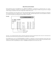
... LOCATION" was changed so that each page is highlighted and displayed in alphabetical order for search with the Acrobat search function. In the circuit diagram section, the symbols (such as @001) indicating internal connections of the Acrobat, but it is positioned in the PDF format, the "TABLE... was eliminated. As an alternative function, the "Signal Location" is mounted and enter the reference number for easy search of the divided circuit diagrams (division numbers) and addresses. It will take time to locate the one you search/display not all pages but the desired page. In ...
... LOCATION" was changed so that each page is highlighted and displayed in alphabetical order for search with the Acrobat search function. In the circuit diagram section, the symbols (such as @001) indicating internal connections of the Acrobat, but it is positioned in the PDF format, the "TABLE... was eliminated. As an alternative function, the "Signal Location" is mounted and enter the reference number for easy search of the divided circuit diagrams (division numbers) and addresses. It will take time to locate the one you search/display not all pages but the desired page. In ...

Service Manual
Page 118
...Correction of Model information table Yes • Correction of BLOCK DIAGRAMS, SCHEMATIC DIAGRAMS, PRINTED WIRING BOARDS • Correction of EXPLODED VIEWS • Correction of Repair Parts List No (DI07-208) HDR-SR5/SR5C/SR5E/SR7/SR7E/SR8/SR8E_L2 Date History Contents S.M. Correction:... Page 5, 3-1, 3-4, 3-5, 3-6, 3-7, 4-1, 4-2, 4-2. SCHMATIC DIAGRAMS 4-33, 4-38, 4-49, 4-72, 5-6, 5-7, 5-8, 5-9, 5-33, ...
...Correction of Model information table Yes • Correction of BLOCK DIAGRAMS, SCHEMATIC DIAGRAMS, PRINTED WIRING BOARDS • Correction of EXPLODED VIEWS • Correction of Repair Parts List No (DI07-208) HDR-SR5/SR5C/SR5E/SR7/SR7E/SR8/SR8E_L2 Date History Contents S.M. Correction:... Page 5, 3-1, 3-4, 3-5, 3-6, 3-7, 4-1, 4-2, 4-2. SCHMATIC DIAGRAMS 4-33, 4-38, 4-49, 4-72, 5-6, 5-7, 5-8, 5-9, 5-33, ...