Programmer Manual
Page 17
... to the RS-232 interface of the ER-A450T to ECR (Auto baud rate setting) X : SSP = 0 Standard RAM (128KB) = 1 Optional RAM: ER-03RA (512KB) = 2 Only nacessary when the ER-01FD or ER-02FD is being used. [JOB#998] RAM data receive Receive from ECR or ER-02FD 998 @/FOR CA/AT (Baud ...the PC. The "02FD.EXE" works with the Windows95/98 operating systems and has the following functions by connecting ER-A450T via RS232. 02FD.EXE : All RAM Data Upload/Download (2) Environment PC and ER-A450T are set as default data. (a) Function text (b) Cashier text (c) Each message text (LOGO, etc..) 5.
... to the RS-232 interface of the ER-A450T to ECR (Auto baud rate setting) X : SSP = 0 Standard RAM (128KB) = 1 Optional RAM: ER-03RA (512KB) = 2 Only nacessary when the ER-01FD or ER-02FD is being used. [JOB#998] RAM data receive Receive from ECR or ER-02FD 998 @/FOR CA/AT (Baud ...the PC. The "02FD.EXE" works with the Windows95/98 operating systems and has the following functions by connecting ER-A450T via RS232. 02FD.EXE : All RAM Data Upload/Download (2) Environment PC and ER-A450T are set as default data. (a) Function text (b) Cashier text (c) Each message text (LOGO, etc..) 5.
Programmer Manual
Page 18
..."Setting" Button." 4 Push "OK" Button. 5 Push "POS -> PC" Button. "Push "Exit" Button." 9 ALL RAM Data Download ( PC -> ER-A450T ) Entry of JOB#996 in the SRV mode 996 6 ER-A450T shows @/FOR CA/AT 00000 UpLoad is shown. Communication starts. 7 UpLoad is completed. 8 The initial Window is completed. 8...mode. And Select the Receiving File. No Procedure on ER-A450T side 2 Place the SRV key in the SRV mode. side Install "02FD.EXE" on the P.C. 1 ALL RAM Data UpLoad : Go to "2" ALL RAM Data DownLoad : Go to "9" 2 ALL RAM Data UpLoad ( ER-A450T -> PC ) "Execute "02FD.EXE" on P.C" ...
..."Setting" Button." 4 Push "OK" Button. 5 Push "POS -> PC" Button. "Push "Exit" Button." 9 ALL RAM Data Download ( PC -> ER-A450T ) Entry of JOB#996 in the SRV mode 996 6 ER-A450T shows @/FOR CA/AT 00000 UpLoad is shown. Communication starts. 7 UpLoad is completed. 8 The initial Window is completed. 8...mode. And Select the Receiving File. No Procedure on ER-A450T side 2 Place the SRV key in the SRV mode. side Install "02FD.EXE" on the P.C. 1 ALL RAM Data UpLoad : Go to "2" ALL RAM Data DownLoad : Go to "9" 2 ALL RAM Data UpLoad ( ER-A450T -> PC ) "Execute "02FD.EXE" on P.C" ...
Service Manual
Page 6
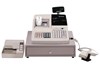
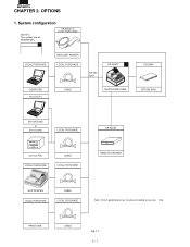
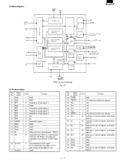
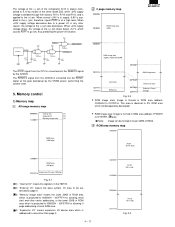
System configuration (NOTE1) This symbol sho ws NEW MODEL ER-A6HS1 or LOCAL PURCHASE LOCAL PURCHASE BARCODE READER LOCAL PURCHASE RS-232 2por t ER-A450T COMPUTER PC UTILITY CABLE MASTER MA CHINE ER-03RA OPTION RAM ER-02FD EXE or ER-01/02FD LOCAL PURCHASE 3.5 inch FDD LOCAL PURCHASE CABLE LOCAL PURCHASE ER-04D W REMOTE DRA WER SLIP PRINTER LOCAL PURCHASE CABLE LOCAL PURCHASE Note : Only 2 peripherals max may be connected at any one time. OPTIONS 1. CHAPTER 2. PRINT DATA CABLE Fig. 1-1 2 - 1
System configuration (NOTE1) This symbol sho ws NEW MODEL ER-A6HS1 or LOCAL PURCHASE LOCAL PURCHASE BARCODE READER LOCAL PURCHASE RS-232 2por t ER-A450T COMPUTER PC UTILITY CABLE MASTER MA CHINE ER-03RA OPTION RAM ER-02FD EXE or ER-01/02FD LOCAL PURCHASE 3.5 inch FDD LOCAL PURCHASE CABLE LOCAL PURCHASE ER-04D W REMOTE DRA WER SLIP PRINTER LOCAL PURCHASE CABLE LOCAL PURCHASE Note : Only 2 peripherals max may be connected at any one time. OPTIONS 1. CHAPTER 2. PRINT DATA CABLE Fig. 1-1 2 - 1
Service Manual
Page 7
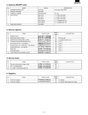
...wire Connector (2pin) 5 TEXT PRESET KEYBOARD COVER PARTS CODE 4. Supplies No. 1 Thermal roll paper 2 Thermal roll paper NAME PARTS CODE DESCRIPTION 512K bytes RAM CHIP FD unit 1 × 1 KEY TOP UNIT 1 × 2 KEY TOP UNIT 2 × 2 KEY TOP UNIT 1 × 1 DUMMY ... CONNECTOR 2 KEY TOP REMOVER 3 2 × 2 KEY TOP INSTALLING JIG PARTS CODE 5. 2. Service tools No. Options (SHARP only) No. NAME 1 EXPANSION RAM CHIP 2 REMOTE DRAWER 3 PRESETS LOADER 4 KEY TOP KIT 5 BARCODE READER MODEL ER-03RA ER-04DW ER-01FD/02FD ER-11KT7 ER-12KT7 ER-22KT7 ER-11DK7G ER-51DK7G ER-A6HS1 3.
...wire Connector (2pin) 5 TEXT PRESET KEYBOARD COVER PARTS CODE 4. Supplies No. 1 Thermal roll paper 2 Thermal roll paper NAME PARTS CODE DESCRIPTION 512K bytes RAM CHIP FD unit 1 × 1 KEY TOP UNIT 1 × 2 KEY TOP UNIT 2 × 2 KEY TOP UNIT 1 × 1 DUMMY ... CONNECTOR 2 KEY TOP REMOVER 3 2 × 2 KEY TOP INSTALLING JIG PARTS CODE 5. 2. Service tools No. Options (SHARP only) No. NAME 1 EXPANSION RAM CHIP 2 REMOTE DRAWER 3 PRESETS LOADER 4 KEY TOP KIT 5 BARCODE READER MODEL ER-03RA ER-04DW ER-01FD/02FD ER-11KT7 ER-12KT7 ER-22KT7 ER-11DK7G ER-51DK7G ER-A6HS1 3.

Service Manual
Page 16
... PWB (PULL UP) Out Chip select base signal for expansion option Out ROM 1 chip select signal Out ROM 2 chip select signal (NU) Out RAM 2 chip select signal Out RAM 1 chip select signal In Printer reset signal In FOR TPRC (NU) +5V Out Printer dot signal 4 (NU) Out Printer dot signal 3 (NU) Out...
... PWB (PULL UP) Out Chip select base signal for expansion option Out ROM 1 chip select signal Out ROM 2 chip select signal (NU) Out RAM 2 chip select signal Out RAM 1 chip select signal In Printer reset signal In FOR TPRC (NU) +5V Out Printer dot signal 4 (NU) Out Printer dot signal 3 (NU) Out...

Service Manual
Page 17
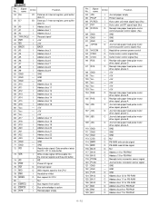
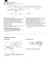
... CG ROM BD0~2 BA0~15 BRD BWR BRAS (BRAS) TPRC1 SO CLOCK SI LATCH ST1~4 HCD PHUP,PSP, PST,POP Thermal head Switch sensor PB RAM (SRAM) Fig. 2-6 The CPU is designed for use with H8/500. However, the thermalhead composition (the dot number and the block number) is not restricted...
... CG ROM BD0~2 BA0~15 BRD BWR BRAS (BRAS) TPRC1 SO CLOCK SI LATCH ST1~4 HCD PHUP,PSP, PST,POP Thermal head Switch sensor PB RAM (SRAM) Fig. 2-6 The CPU is designed for use with H8/500. However, the thermalhead composition (the dot number and the block number) is not restricted...
Service Manual
Page 19
... 12 GND 13 GND 14 SI 15 SO 16 CLOCK 17 INHDEC In/Out Function - TPRC1 O Send data from TPRC1 to thermalhead Data from PB-RAM or zero data are outputted at the falling of CLOCK signal. 16 O Thermalhead CLOCK signal SO is outputted at the edge of I Ä O, and is...
... 12 GND 13 GND 14 SI 15 SO 16 CLOCK 17 INHDEC In/Out Function - TPRC1 O Send data from TPRC1 to thermalhead Data from PB-RAM or zero data are outputted at the falling of CLOCK signal. 16 O Thermalhead CLOCK signal SO is outputted at the edge of I Ä O, and is...
Service Manual
Page 20
...GND 71 GND - GND 72 RD I Journal motor connector sensor signal - GND - GND O NU O PB-RAM write strobe signal O PB-RAM read strobe signal O NU O Address 14 for PB-RAM O Address 13 for PB-RAM 4 - 12 NU 81 EBREQ I Bus request from option 82 EBACK O Bus acknowledge to option 83 RPE I... motor drive signal, phase A - GND O GND O Address bus 12 for PB-RAM O Address bus 11 for PB-RAM O Address bus 10 for PB-RAM O Address bus 9 for PB-RAM O Address bus 8 for PB-RAM O Address bus 7 for PB-RAM I Receipt motor connector sensor signal I Read strobe signal: Gate enable of data bus D0...
...GND 71 GND - GND 72 RD I Journal motor connector sensor signal - GND - GND O NU O PB-RAM write strobe signal O PB-RAM read strobe signal O NU O Address 14 for PB-RAM O Address 13 for PB-RAM 4 - 12 NU 81 EBREQ I Bus request from option 82 EBACK O Bus acknowledge to option 83 RPE I... motor drive signal, phase A - GND O GND O Address bus 12 for PB-RAM O Address bus 11 for PB-RAM O Address bus 10 for PB-RAM O Address bus 9 for PB-RAM O Address bus 8 for PB-RAM O Address bus 7 for PB-RAM I Receipt motor connector sensor signal I Read strobe signal: Gate enable of data bus D0...

Service Manual
Page 21
...GND O Address bus 6 for PB-RAM O Address bus 5 for PB-RAM O Address bus 4 for PB-RAM O Address bus 3 for PB-RAM O Address bus 2 for PB-RAM O Address bus 1 for PB-RAM I /O Data bus 3 for PB-RAM 2-5. GND - OPC2 1) Pin configuration Pin Signal No. GND I/O Data bus 4 for PB-RAM I TPRC1 clock input pin (9.83 ... Function I/O Data bus 7 for PB-RAM I/O Data bus 6 for PB-RAM - GND I/O Data bus 2 for PB-RAM I/O Data bus 1 for PB-RAM I/O Data bus 0 for PB-RAM O PB-RAM chip select: Active HIGH (Nu) O PB-RAM chip select: Active LOW I /O Data bus 5 for PB-RAM I TPRC1 reset signal - Pin Signal ...
...GND O Address bus 6 for PB-RAM O Address bus 5 for PB-RAM O Address bus 4 for PB-RAM O Address bus 3 for PB-RAM O Address bus 2 for PB-RAM O Address bus 1 for PB-RAM I /O Data bus 3 for PB-RAM 2-5. GND - OPC2 1) Pin configuration Pin Signal No. GND I/O Data bus 4 for PB-RAM I TPRC1 clock input pin (9.83 ... Function I/O Data bus 7 for PB-RAM I/O Data bus 6 for PB-RAM - GND I/O Data bus 2 for PB-RAM I/O Data bus 1 for PB-RAM I/O Data bus 0 for PB-RAM O PB-RAM chip select: Active HIGH (Nu) O PB-RAM chip select: Active LOW I /O Data bus 5 for PB-RAM I TPRC1 reset signal - Pin Signal ...
Service Manual
Page 24
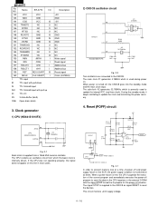
... which is internally driven. The main clock X1 generates 4.19MHz which the basic clock is primarily used during power on this line in the external S-RAM with pull up TTL I TTL input TTL input with pull down TTL Schmidt input TTL Schmidt input with the signal STOP forced low to update... 143 144 145 146 147 148 149 150 151 152 153 154 155 156 157 158 159 160 I ID IS ISU IO 3S ON6 Name ER-A770 I/O VCC VCC GND GND /CSD VCC IS TRNDTD NC O /DTRD NC O /RTSD NC O RCVDTD GND IS /CTSD GND IS /DSRD GND IS TRNRDYD NC...
... which is internally driven. The main clock X1 generates 4.19MHz which the basic clock is primarily used during power on this line in the external S-RAM with pull up TTL I TTL input TTL input with pull down TTL Schmidt input TTL Schmidt input with the signal STOP forced low to update... 143 144 145 146 147 148 149 150 151 152 153 154 155 156 157 158 159 160 I ID IS ISU IO 3S ON6 Name ER-A770 I/O VCC VCC GND GND /CSD VCC IS TRNDTD NC O /DTRD NC O /RTSD NC O RCVDTD GND IS /CTSD GND IS /DSRD GND IS TRNRDYD NC...
Service Manual
Page 25
When +24V supply voltage drops, the voltage at the (+) pin drops below +5.1V, which will beseparately developed. • RAM image area: Image is formed in RAM area address 1F0000H to 1F7E7FH. ( Note) Note: Image can be addressed in supply, 6.8V is supplied to the (+) pin, therefore, signal POFF is... C86 1000P VDD 14 4 6 5 IC12B 74HC00S /RESET /(RAS3./RESET) C175 1000P The STOP signal from the CKDC8 is formed in lower 32KB of work RAM area. ( 4) "Expansion I/O" means expansion I/O device area which is projected to 5.1V by means of the zener diode ZD2, while +24V supply voltage ...
When +24V supply voltage drops, the voltage at the (+) pin drops below +5.1V, which will beseparately developed. • RAM image area: Image is formed in RAM area address 1F0000H to 1F7E7FH. ( Note) Note: Image can be addressed in supply, 6.8V is supplied to the (+) pin, therefore, signal POFF is... C86 1000P VDD 14 4 6 5 IC12B 74HC00S /RESET /(RAS3./RESET) C175 1000P The STOP signal from the CKDC8 is formed in lower 32KB of work RAM area. ( 4) "Expansion I/O" means expansion I/O device area which is projected to 5.1V by means of the zener diode ZD2, while +24V supply voltage ...
Service Manual
Page 26
...as OR in the image area of no stack process immediately after resetting. 4 - 18 Note 2: OPCCS1 and OPCCS2 signals are decoded in the ER-A445P. (Not used) Access is selected for initializing.) : For 0 page image area, selection between RAS2 and RAS3 can bemade with two ROM...MCR2 (NOT USE) (*2) OPCCS1 (*2) OPCCS2 NOT USE NOT USE NOT USE Fig. 5-5 Note 1: MPCCS signal is performed with two RAM chip select signals, RAS2 and RAS3. RAM control Address A23~A14 200000H~3FFFFFH 1C0000H~1DFFFFH Address decorder 008000H~ 00F7FFH *1 1E0000H~1FFFFFH RAS3 RAS1 RAS2 DOI D Q Control register S8F...
...as OR in the image area of no stack process immediately after resetting. 4 - 18 Note 2: OPCCS1 and OPCCS2 signals are decoded in the ER-A445P. (Not used) Access is selected for initializing.) : For 0 page image area, selection between RAS2 and RAS3 can bemade with two ROM...MCR2 (NOT USE) (*2) OPCCS1 (*2) OPCCS2 NOT USE NOT USE NOT USE Fig. 5-5 Note 1: MPCCS signal is performed with two RAM chip select signals, RAS2 and RAS3. RAM control Address A23~A14 200000H~3FFFFFH 1C0000H~1DFFFFH Address decorder 008000H~ 00F7FFH *1 1E0000H~1FFFFFH RAS3 RAS1 RAS2 DOI D Q Control register S8F...

Service Manual
Page 27
... for "-----." 3 Lower bits 4 Enable register EN (bit7) = 1 Enable = 0 Inhibit < BAR composition > Fig. 6-4 is accessed through the address FFFF00H or later decoded in the conventional monitor RAM. In the exception process routine of the service routine, the entry address is performed through the direct address of the break address are assigned to...
... for "-----." 3 Lower bits 4 Enable register EN (bit7) = 1 Enable = 0 Inhibit < BAR composition > Fig. 6-4 is accessed through the address FFFF00H or later decoded in the conventional monitor RAM. In the exception process routine of the service routine, the entry address is performed through the direct address of the break address are assigned to...
Service Manual
Page 28
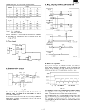
... thermal printer controller (TPRC1). Therefore any unnecessary read . If there are read access in the NMI sub routine. (Clear by reading address FFFFFFH (*1). The PB-RAM connected to TPRC1 serves as the paper feed motor. • Drive sequence of each break address register. PRINTER control circuit 1) Block diagram RECEIVER CPU Address...
... thermal printer controller (TPRC1). Therefore any unnecessary read . If there are read access in the NMI sub routine. (Clear by reading address FFFFFFH (*1). The PB-RAM connected to TPRC1 serves as the paper feed motor. • Drive sequence of each break address register. PRINTER control circuit 1) Block diagram RECEIVER CPU Address...
Service Manual
Page 29
... directly supported by turning on sequence During service interruption, the CKDC8 senses POF within 500msec. is connected to the CPU through MPCA6. 3) Print circuit PB RAM STRB1~STRB5 TPRC 1 LATCH SO SI CLOCK VHCOM Thermal printer head VRES VH +24V 8. POF RES1 SHEN LDRQ 1 2 Start condition Next command Fig. 9-2 After sampling...
... directly supported by turning on sequence During service interruption, the CKDC8 senses POF within 500msec. is connected to the CPU through MPCA6. 3) Print circuit PB RAM STRB1~STRB5 TPRC 1 LATCH SO SI CLOCK VHCOM Thermal printer head VRES VH +24V 8. POF RES1 SHEN LDRQ 1 2 Start condition Next command Fig. 9-2 After sampling...
Service Manual
Page 31
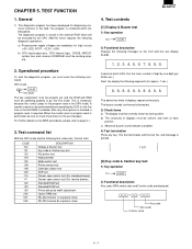
... width adjustment Option RAM test RS-232 channel 1 Loop back check RS-232 channel 8 Loop back check 4. and message is printed 1 0 0 [2] Key code & Cashier key test 1) Key operation 101 CA/AT 2) Functional description Key code, MRS switch state and Cashier code are mandatory for the first time or the ER-03RA is...
... width adjustment Option RAM test RS-232 channel 1 Loop back check RS-232 channel 8 Loop back check 4. and message is printed 1 0 0 [2] Key code & Cashier key test 1) Key operation 101 CA/AT 2) Functional description Key code, MRS switch state and Cashier code are mandatory for the first time or the ER-03RA is...
Service Manual
Page 34
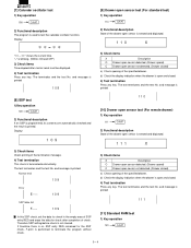
... of the drawer open sensor is open and closed . 4) Test termination Press any key. The test terminates and the test No. "-" is printed 1 1 1 [11] Standard RAM test 1) Key operation 120 CA/AT 5 - 4 [7] Calendar oscillator test 1) Key operation 108 CA/AT 2) Functional description This program is open and closed . 4) Test termination Press...
... of the drawer open sensor is open and closed . 4) Test termination Press any key. The test terminates and the test No. "-" is printed 1 1 1 [11] Standard RAM test 1) Key operation 120 CA/AT 5 - 4 [7] Calendar oscillator test 1) Key operation 108 CA/AT 2) Functional description This program is open and closed . 4) Test termination Press...
Service Manual
Page 35
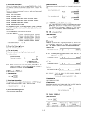
...test 1) Key operation 151 CA/AT 2) Contents The digital conversion value of SUM is 10H, it is performed further. Option RAM Memory to be checked ER-03RA Address area to be changed before and after the check. intervals by a timer control and is displayed sequentially. Perform the... following processes for the standard RAM 256 KByte SRAM. PASS5: Read and compare data "AAAAH." Check point address = 1C0000H, 1C0001H,...
...test 1) Key operation 151 CA/AT 2) Contents The digital conversion value of SUM is 10H, it is performed further. Option RAM Memory to be checked ER-03RA Address area to be changed before and after the check. intervals by a timer control and is displayed sequentially. Perform the... following processes for the standard RAM 256 KByte SRAM. PASS5: Read and compare data "AAAAH." Check point address = 1C0000H, 1C0001H,...
Service Manual
Page 38
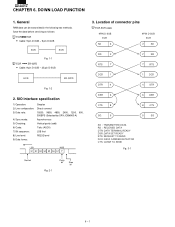
... level: RS232 level 9) Data forma: LSB MSB b1 b2 b3 b4 b5 b6 b7 P Start bit FIg. 2-1 Parity bit Stop bit 3. DOWN LOAD FUNCTION 1. General RAM data can be transmitted in the following two methods. Save the data before servicing as follows: ECR ECR • Cable: 9 pin D-SUB - 9 pin D-SUB ECR...
... level: RS232 level 9) Data forma: LSB MSB b1 b2 b3 b4 b5 b6 b7 P Start bit FIg. 2-1 Parity bit Stop bit 3. DOWN LOAD FUNCTION 1. General RAM data can be transmitted in the following two methods. Save the data before servicing as follows: ECR ECR • Cable: 9 pin D-SUB - 9 pin D-SUB ECR...
Service Manual
Page 39
... be transmitted is connected to ECR only) 5. Page:1F ∼ 27,00 Page of RAM memory may avoid over-riding pages for this job, the RAM image is sent in unit of the cable. ECR-ER-02FD cable 25PIN D-SUB ER-02FD SD 2 9PIN D-SUB ECR 3 SD RD 3 RTS 4 DCD 8 2 RD 7 ...RTS 1 DCD DTR 20 4 DTR DSR 6 6 DSR CTS 5 8 CTS SG 7 5 SG FG 1 FRAME GROUND is divided into a high order 4 bits and low order 4 bits and converted into ASCII code. RAM DATA FORMAT...
... be transmitted is connected to ECR only) 5. Page:1F ∼ 27,00 Page of RAM memory may avoid over-riding pages for this job, the RAM image is sent in unit of the cable. ECR-ER-02FD cable 25PIN D-SUB ER-02FD SD 2 9PIN D-SUB ECR 3 SD RD 3 RTS 4 DCD 8 2 RD 7 ...RTS 1 DCD DTR 20 4 DTR DSR 6 6 DSR CTS 5 8 CTS SG 7 5 SG FG 1 FRAME GROUND is divided into a high order 4 bits and low order 4 bits and converted into ASCII code. RAM DATA FORMAT...


