Product Manual
Page 19
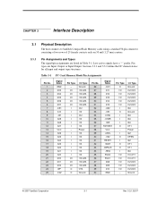
... host connects to SanDisk CompactFlash Memory cards using a standard 50-pin connector consisting of two rows of 25 female contacts each on 50 mil (1.27 mm) centers. 3.1.1 Pin Assignments and Types The signal/pin assignments are Input, Output or Input/Output. Low active signals have a "-" prefix. Table 3-1 PC Card Memory Mode Pin Assignments ...Pin No. 1 2 3 4 5 6 7 8 9 10 11 12 13 14 15 16 17 18 19 20 21 22 23 24 25 Signal Name GND D03 D04 D05 D06 D07 -CE1 A10 -OE A09 A08 A07 VCC A06 A05 A04 A03 A02...
... host connects to SanDisk CompactFlash Memory cards using a standard 50-pin connector consisting of two rows of 25 female contacts each on 50 mil (1.27 mm) centers. 3.1.1 Pin Assignments and Types The signal/pin assignments are Input, Output or Input/Output. Low active signals have a "-" prefix. Table 3-1 PC Card Memory Mode Pin Assignments ...Pin No. 1 2 3 4 5 6 7 8 9 10 11 12 13 14 15 16 17 18 19 20 21 22 23 24 25 Signal Name GND D03 D04 D05 D06 D07 -CE1 A10 -OE A09 A08 A07 VCC A06 A05 A04 A03 A02...
Product Manual
Page 20
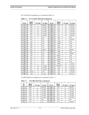
... I O I I I /O Type Ground I1Z,OZ3 I1Z,OZ3 I1Z,OZ3 I1Z,OZ3 I1Z,OZ3 I3Z Ground 02/07, Rev. 12.0 3-2 © 2007 SanDisk Corporation Ground 26 2 D03 I/O I1Z,OZ3 27 3 D04 I/O I1Z,OZ3 28 4 D05 I/O I1Z,OZ3 29 5 D06 I/O I1Z,OZ3 30 6 D07 ... Type I /O Mode Pin Assignments Signal Name GND D03 D04 D05 D06 D07 -CE1 A10 -OE A09 A08 A07 VCC A06 A05 A04 A03 A02 A01 A00 D00 D01 D02 -IOIS16 -CD2 Pin Type - Interface Description SanDisk CompactFlash Card OEM Product Manual PC Card I/O Pin Assignments are contained in Table 3-2. I/O I/O I/O I/O I/O I I I I I I /O - ...
... I O I I I /O Type Ground I1Z,OZ3 I1Z,OZ3 I1Z,OZ3 I1Z,OZ3 I1Z,OZ3 I3Z Ground 02/07, Rev. 12.0 3-2 © 2007 SanDisk Corporation Ground 26 2 D03 I/O I1Z,OZ3 27 3 D04 I/O I1Z,OZ3 28 4 D05 I/O I1Z,OZ3 29 5 D06 I/O I1Z,OZ3 30 6 D07 ... Type I /O Mode Pin Assignments Signal Name GND D03 D04 D05 D06 D07 -CE1 A10 -OE A09 A08 A07 VCC A06 A05 A04 A03 A02 A01 A00 D00 D01 D02 -IOIS16 -CD2 Pin Type - Interface Description SanDisk CompactFlash Card OEM Product Manual PC Card I/O Pin Assignments are contained in Table 3-2. I/O I/O I/O I/O I/O I I I I I I /O - ...
Product Manual
Page 22
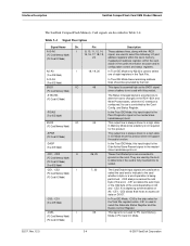
.... Interface Description SanDisk CompactFlash Card OEM Product Manual The SanDisk CompactFlash Memory Card signals are used to select the following: I/O port address registers within the card, memorymapped port address registers within the card, a byte in the card's information structure and its socket. -CE1, -CE2 I (PC Card Memory Mode) (PC Card I/O Mode) 7, 32 The Card Enable input signals are used by the Card Config. A10-A3 (True...
.... Interface Description SanDisk CompactFlash Card OEM Product Manual The SanDisk CompactFlash Memory Card signals are used to select the following: I/O port address registers within the card, memorymapped port address registers within the card, a byte in the card's information structure and its socket. -CE1, -CE2 I (PC Card Memory Mode) (PC Card I/O Mode) 7, 32 The Card Enable input signals are used by the Card Config. A10-A3 (True...
Product Manual
Page 39
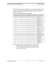
... status information about the card that have alternate use in future products. SanDisk CompactFlash Card OEM Product Manual Interface Description In addition, these locations may be performed to the card attribute memory except to replace status ... registers should be used to arbitrate between multiple interrupt sources on dedicated pins in memory cards that may vary in I/O cards. bit D7-D0) 0 1 1 1 0 X X XX X X X X Common Memory Write (8- Table 3-17 Registers and Memory Space Decoding A8-CE2 -CE1 -REG -OE -WE A10 A9 A4 A3 A2 A1 A0 Selected Space 1 1 X X X X X ...
... status information about the card that have alternate use in future products. SanDisk CompactFlash Card OEM Product Manual Interface Description In addition, these locations may be performed to the card attribute memory except to replace status ... registers should be used to arbitrate between multiple interrupt sources on dedicated pins in memory cards that may vary in I/O cards. bit D7-D0) 0 1 1 1 0 X X XX X X X X Common Memory Write (8- Table 3-17 Registers and Memory Space Decoding A8-CE2 -CE1 -REG -OE -WE A10 A9 A4 A3 A2 A1 A0 Selected Space 1 1 X X X X X ...
Product Manual
Page 40
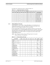
.../07, Rev. 12.0 3-22 © 2007 SanDisk Corporation Table 3-18 Configuration Registers Decoding A8-CE2 -CE1 -REG -OE -WE A10 A9 A4 A3 A2 A1 A0 Selected Register X ...Memory Function Attribute Memory is a space where a CompactFlash Memory Card identification and configuration information is stored, and is limited to Table 3-19 for signal states and bus validity for the configuration registers is valid during the cycle. The card configuration registers are also located there. Refer to 8-bit wide accesses only at even addresses. Interface Description SanDisk CompactFlash Card...
.../07, Rev. 12.0 3-22 © 2007 SanDisk Corporation Table 3-18 Configuration Registers Decoding A8-CE2 -CE1 -REG -OE -WE A10 A9 A4 A3 A2 A1 A0 Selected Register X ...Memory Function Attribute Memory is a space where a CompactFlash Memory Card identification and configuration information is stored, and is limited to Table 3-19 for signal states and bus validity for the configuration registers is valid during the cycle. The card configuration registers are also located there. Refer to 8-bit wide accesses only at even addresses. Interface Description SanDisk CompactFlash Card...

Product Manual
Page 47
... low (and A0 = Do not care) as byte register with -CE1 low and -CE2 high. SanDisk CompactFlash Card OEM Product Manual ATA Register Set and Protocol 4.3 Memory Mapped Addressing When CompactFlash Memory Card registers are not supported. Table 4-4 Memory Mapped Decoding A9-REG A10 A4 A3 A2 A1 A0 Offset -OE=0 -WE=0 1 0 X 0 0 0 0 0 Even RD Dataa Even WR ...or feature (write) register. Some PCMCIA socket adapters also have auto incrementing address logic embedded within the card. © 2007 SanDisk Corporation 4-3 Rev. 12.0, 02/07 Accesses to function efficiently.
... low (and A0 = Do not care) as byte register with -CE1 low and -CE2 high. SanDisk CompactFlash Card OEM Product Manual ATA Register Set and Protocol 4.3 Memory Mapped Addressing When CompactFlash Memory Card registers are not supported. Table 4-4 Memory Mapped Decoding A9-REG A10 A4 A3 A2 A1 A0 Offset -OE=0 -WE=0 1 0 X 0 0 0 0 0 Even RD Dataa Even WR ...or feature (write) register. Some PCMCIA socket adapters also have auto incrementing address logic embedded within the card. © 2007 SanDisk Corporation 4-3 Rev. 12.0, 02/07 Accesses to function efficiently.
