Data Sheet
Page 1
Intel® Core™2 Duo Mobile Processor, Intel® Core™2 Solo Mobile Processor and Intel® Core™2 Extreme Mobile Processor on 45-nm Process Datasheet For platforms based on Mobile Intel® 4 Series Express Chipset Family March 2009 Document Number: 320120-004
Intel® Core™2 Duo Mobile Processor, Intel® Core™2 Solo Mobile Processor and Intel® Core™2 Extreme Mobile Processor on 45-nm Process Datasheet For platforms based on Mobile Intel® 4 Series Express Chipset Family March 2009 Document Number: 320120-004

Data Sheet
Page 2
...request. Intel, Pentium, Centrino, Intel Core Duo, Intel SpeedStep, MMX and the Intel logo are trademarks of others. Designers must not rely on the absence or characteristics of this processor are ...available on hardware and software configurations and may contain design defects or errors known as the property of Intel Corporation in this information. The products described in the U.S. Check with a processor, chipset...
...request. Intel, Pentium, Centrino, Intel Core Duo, Intel SpeedStep, MMX and the Intel logo are trademarks of others. Designers must not rely on the absence or characteristics of this processor are ...available on hardware and software configurations and may contain design defects or errors known as the property of Intel Corporation in this information. The products described in the U.S. Check with a processor, chipset...

Data Sheet
Page 7
...-level, shared cache with Advanced Transfer Cache architecture • The processor in ULV single-core and dual-core have an on the Intel Core microarchitecture for : - Key features include: • Dual-core processor for the following processors: • The Intel Core 2 Duo processors and Intel Core 2 Extreme processors support the Mobile Intel® 4 Series Express Chipset and Intel® ICH9M I /O controller. This document contains electrical, mechanical and thermal...
...-level, shared cache with Advanced Transfer Cache architecture • The processor in ULV single-core and dual-core have an on the Intel Core microarchitecture for : - Key features include: • Dual-core processor for the following processors: • The Intel Core 2 Duo processors and Intel Core 2 Extreme processors support the Mobile Intel® 4 Series Express Chipset and Intel® ICH9M I /O controller. This document contains electrical, mechanical and thermal...
Data Sheet
Page 8
...are offered in Micro-FCBGA packaging technologies only • Execute Disable Bit support for core to bus ratio Terminology Term # Front Side Bus (FSB) AGTL+ Storage Conditions Enhanced Intel SpeedStep® Technology Processor Core Definition A "#" symbol after a signal name refers to free air. In the ...POP, LV and ULV are at the pads of a binary sequence (such as the chipset components). Upon exposure to "free air" (i.e., unsealed packaging or a device removed from packaging material) the processor must be installed in a platform, in packaging or exposed to an active low signal,...
...are offered in Micro-FCBGA packaging technologies only • Execute Disable Bit support for core to bus ratio Terminology Term # Front Side Bus (FSB) AGTL+ Storage Conditions Enhanced Intel SpeedStep® Technology Processor Core Definition A "#" symbol after a signal name refers to free air. In the ...POP, LV and ULV are at the pads of a binary sequence (such as the chipset components). Upon exposure to "free air" (i.e., unsealed packaging or a device removed from packaging material) the processor must be installed in a platform, in packaging or exposed to an active low signal,...

Data Sheet
Page 9
... marked as executable or nonexecutable, when combined with a supporting operating system. Document Intel® Core™2 Duo Mobile Processor, Intel® Core™2 Solo Mobile Processor, Intel® Core™2 Extreme Processor on 45-nm Technology Specification Update Mobile Intel® 4 Series Express Chipset Family Datasheet Mobile Intel® 4 Series Express Chipset Family Specification Update Intel® I/O Controller Hub 9 (ICH9)/ I/O Controller Hub 9M (ICH9M) Datasheet...
... marked as executable or nonexecutable, when combined with a supporting operating system. Document Intel® Core™2 Duo Mobile Processor, Intel® Core™2 Solo Mobile Processor, Intel® Core™2 Extreme Processor on 45-nm Technology Specification Update Mobile Intel® 4 Series Express Chipset Family Datasheet Mobile Intel® 4 Series Express Chipset Family Specification Update Intel® I/O Controller Hub 9 (ICH9)/ I/O Controller Hub 9M (ICH9M) Datasheet...
Data Sheet
Page 17
... • Once the L2 cache has been reduced to zero, the processor triggers a special chipset sequence to notify the chipset to redirect all the caches are directed to the Intel Enhanced Deeper Sleep state core voltage on reducing the L2 cache and entering Intel Enhanced Deeper Sleep state. The snoops are replied as all FSB traffic...
... • Once the L2 cache has been reduced to zero, the processor triggers a special chipset sequence to notify the chipset to redirect all the caches are directed to the Intel Enhanced Deeper Sleep state core voltage on reducing the L2 cache and entering Intel Enhanced Deeper Sleep state. The snoops are replied as all FSB traffic...
Data Sheet
Page 29
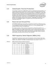
...inputs should be turned off within 500 ms to prevent permanent silicon damage due to the clock chip and the appropriate chipset on the processor silicon. BSEL[2:0] Encoding for catastrophic thermal protection. THERMTRIP# functionality is not ensured if the PWRGOOD signal is asserted, the...left as no-connects if AGTL+ termination is shown in component malfunction or incompatibility with the activation of THERMTRIP#, which halts all processor internal clocks and activity, leakage current can be left unconnected. Unused active low AGTL+ inputs may be left as "No Connects"....
...inputs should be turned off within 500 ms to prevent permanent silicon damage due to the clock chip and the appropriate chipset on the processor silicon. BSEL[2:0] Encoding for catastrophic thermal protection. THERMTRIP# functionality is not ensured if the PWRGOOD signal is asserted, the...left as no-connects if AGTL+ termination is shown in component malfunction or incompatibility with the activation of THERMTRIP#, which halts all processor internal clocks and activity, leakage current can be left unconnected. Unused active low AGTL+ inputs may be left as "No Connects"....
Data Sheet
Page 94
...new requests, unless such requests are part of the signals and the frequency associated with each combination. D[63:0]# are used by the processor, chipset and clock synthesizer. The data bus is released after DBSY# is inverted and therefore sampled active high. This signal must connect the ...defines the possible combinations of an ongoing locked operation. Each group of one DSTBP# and one DINV# signal. DBR# is determined by the processor to indicate that an in-target probe can drive system reset. DBSY# (Data Bus Busy) is asserted by a debug port interposer so ...
...new requests, unless such requests are part of the signals and the frequency associated with each combination. D[63:0]# are used by the processor, chipset and clock synthesizer. The data bus is released after DBSY# is inverted and therefore sampled active high. This signal must connect the ...defines the possible combinations of an ongoing locked operation. Each group of one DSTBP# and one DINV# signal. DBR# is determined by the processor to indicate that an in-target probe can drive system reset. DBSY# (Data Bus Busy) is asserted by a debug port interposer so ...
Data Sheet
Page 95
...signal used to reduce power on the data bus. In a multi-common clock data transfer, DRDY# may be deasserted. DPRSTP# is asserted by the chipset to latch in D[63:0]#. DSTBN[3:0]# Input/ Output Signals Associated Strobe D[15:0]#, DINV[0]# D[31:16]#, DINV[1]# DSTBN[0]# DSTBN[1]# D[47:32]#, DINV...next cycle. The DINV[3:0]# signals are source synchronous and indicate the polarity of both FSB agents. DPSLP# is inverted. The processor drives this pin during dynamic FSB frequency switching. Assertion of DEFER# is normally the responsibility of both FSB agents. The ...
...signal used to reduce power on the data bus. In a multi-common clock data transfer, DRDY# may be deasserted. DPRSTP# is asserted by the chipset to latch in D[63:0]#. DSTBN[3:0]# Input/ Output Signals Associated Strobe D[15:0]#, DINV[0]# D[31:16]#, DINV[1]# DSTBN[0]# DSTBN[1]# D[47:32]#, DINV...next cycle. The DINV[3:0]# signals are source synchronous and indicate the polarity of both FSB agents. DPSLP# is inverted. The processor drives this pin during dynamic FSB frequency switching. Assertion of DEFER# is normally the responsibility of both FSB agents. The ...