Hard Drive Specifications
Page 6
...43 6.7.3 Seek/ID Mis-compare Errors 43 6.7.4 Equipment Errors 43 6.7.5 Failure Prediction ( PFA / S.M.A.R.T 43 6.7.6 Automatic Drive Maintenance (ADM 44 6.7.7 Preventive Maintenance 44 6.8 Mechanical Specifications 45 6.8.1 Outline 45 6.8.2 Mechanical Dimensions 48 6.8.3 Interface Connector...Flammability 59 6.13.6 Secondary Circuit Protection 59 6.14 Packaging 59 Part 2. EVPD = 0 72 7.6.2 Inquiry Data Format - of DDRS-3xxxx Page Code = 00 74 iv O E M Spec. EVPD = 1 - SCSI Interface Specification 61 7.0 SCSI COMMAND SET 63 7.1 Flag and Link Bits 64 7.2 Abbreviations 65 ...
...43 6.7.3 Seek/ID Mis-compare Errors 43 6.7.4 Equipment Errors 43 6.7.5 Failure Prediction ( PFA / S.M.A.R.T 43 6.7.6 Automatic Drive Maintenance (ADM 44 6.7.7 Preventive Maintenance 44 6.8 Mechanical Specifications 45 6.8.1 Outline 45 6.8.2 Mechanical Dimensions 48 6.8.3 Interface Connector...Flammability 59 6.13.6 Secondary Circuit Protection 59 6.14 Packaging 59 Part 2. EVPD = 0 72 7.6.2 Inquiry Data Format - of DDRS-3xxxx Page Code = 00 74 iv O E M Spec. EVPD = 1 - SCSI Interface Specification 61 7.0 SCSI COMMAND SET 63 7.1 Flag and Link Bits 64 7.2 Abbreviations 65 ...

Hard Drive Specifications
Page 8
... 10.1.1 Priority of SCSI Status Byte Reporting 179 10.1.2 Invalid L U N in Identify Message 179 10.1.3 Incorrect Initiator Connection 180 10.1.4 Command Processing During Execution of DDRS-3xxxx 7.32 SYNCHRONIZE CACHE (35 148 7.33 TEST UNIT READY (00 149 7.34 VERIFY (2F 150 7.35 WRITE (0A 151 7.36 WRITE E X T E N D E D (2A 152 7.37... (0D 171 9.1.16 CLEAR QUEUE TAG (0E 171 9.1.17 QUEUE TAG MESSAGES(20h, 21h, 22h 171 9.1.18 I /O process 180 10.1.5 Unit Attention Condition 183 vi O E M Spec.
... 10.1.1 Priority of SCSI Status Byte Reporting 179 10.1.2 Invalid L U N in Identify Message 179 10.1.3 Incorrect Initiator Connection 180 10.1.4 Command Processing During Execution of DDRS-3xxxx 7.32 SYNCHRONIZE CACHE (35 148 7.33 TEST UNIT READY (00 149 7.34 VERIFY (2F 150 7.35 WRITE (0A 151 7.36 WRITE E X T E N D E D (2A 152 7.37... (0D 171 9.1.16 CLEAR QUEUE TAG (0E 171 9.1.17 QUEUE TAG MESSAGES(20h, 21h, 22h 171 9.1.18 I /O process 180 10.1.5 Unit Attention Condition 183 vi O E M Spec.

Hard Drive Specifications
Page 10
12.2.4 Sense Key (Bit 3 - 0 of DDRS-3xxxx of byte 2 206 12.2.5 Information Bytes (Byte 3 thru 6 207 12.2.6 Additional Sense Length (Byte 7 207 12.2.7 Command Specific Information (Byte 8 thru 11 207 12.2.8 Additional Sense Code/Qualifier (Byte 12 and 13 208 12.2.9 F R U : Field Replaceable Unit (Byte 14 211 12.2.10 Sense Key Specific (Byte 15 thru 17 211 12.2.11 Reserved (Byte 18 thru 19 212 12.2.12 Vender unique error information (Byte 20 thru 23 213 12.2.13 Physical Error Record (Byte 24 thru 29 213 12.2.14 Reserved (Byte 30 thru 31 213 Index 215 viii OEM Spec.
12.2.4 Sense Key (Bit 3 - 0 of DDRS-3xxxx of byte 2 206 12.2.5 Information Bytes (Byte 3 thru 6 207 12.2.6 Additional Sense Length (Byte 7 207 12.2.7 Command Specific Information (Byte 8 thru 11 207 12.2.8 Additional Sense Code/Qualifier (Byte 12 and 13 208 12.2.9 F R U : Field Replaceable Unit (Byte 14 211 12.2.10 Sense Key Specific (Byte 15 thru 17 211 12.2.11 Reserved (Byte 18 thru 19 212 12.2.12 Vender unique error information (Byte 20 thru 23 213 12.2.13 Physical Error Record (Byte 24 thru 29 213 12.2.14 Reserved (Byte 30 thru 31 213 Index 215 viii OEM Spec.

Hard Drive Specifications
Page 12
1.3 Glossary Word Kbpi Mbps | GB MB KB 32KB 64KB Mb/sq.in MLC PFA S.M.A.R.T. of the ESD protective bag are the user's responsibility. 2 OEM Spec. ADM SCAM | SE | LVD Meaning 1,000 Bits Per Inch 1,000,000 Bits per second 1,000,000,000 bytes ...per square inch Machine Level Control Predictive Failure Analysis (Trademark of IBM Corp.) Self-Monitoring Analysis and Reporting Technology Automatic Drive Maintenance SCSI Configured AutoMatically Single Ended SCSI Low Voltage Differential SCSI 1.4 General Caution The drive can be easily damaged by shocks or ESD (Electric Static ...
1.3 Glossary Word Kbpi Mbps | GB MB KB 32KB 64KB Mb/sq.in MLC PFA S.M.A.R.T. of the ESD protective bag are the user's responsibility. 2 OEM Spec. ADM SCAM | SE | LVD Meaning 1,000 Bits Per Inch 1,000,000 Bits per second 1,000,000,000 bytes ...per square inch Machine Level Control Predictive Failure Analysis (Trademark of IBM Corp.) Self-Monitoring Analysis and Reporting Technology Automatic Drive Maintenance SCSI Configured AutoMatically Single Ended SCSI Low Voltage Differential SCSI 1.4 General Caution The drive can be easily damaged by shocks or ESD (Electric Static ...

Hard Drive Specifications
Page 20
...(Format Device Parameters) and 0C (Notch Parameters) provide methods to drive performance. There are other parameters that contribute to the performance of DDRS-3xxxx of the actual system. This specification tries to define the bare drive characteristics, not the system throughput which will depend on page 110... "Page 3 (Format Device Parameters)" on page 102, and 7.9.11, "Page 0C (Notch Parameters)" on the system and the application. 10 OEM Spec. 3.3 Cylinder Allocation System Area Data Zone 0 Data Zone 1 Data Zone 2 Data Zone 3 Data Zone 4 Data Zone 5 Data Zone 6 Data Zone 7...
...(Format Device Parameters) and 0C (Notch Parameters) provide methods to drive performance. There are other parameters that contribute to the performance of DDRS-3xxxx of the actual system. This specification tries to define the bare drive characteristics, not the system throughput which will depend on page 110... "Page 3 (Format Device Parameters)" on page 102, and 7.9.11, "Page 0C (Notch Parameters)" on the system and the application. 10 OEM Spec. 3.3 Cylinder Allocation System Area Data Zone 0 Data Zone 1 Data Zone 2 Data Zone 3 Data Zone 4 Data Zone 5 Data Zone 6 Data Zone 7...

Hard Drive Specifications
Page 22
... after reading the last sector in 3.4.7, "Throughput" on page 15. 3.4.2.4 Head Switch Time (Head Skew) Figure 7. The measured method is defined as the average of DDRS-3xxxx of 1000 full stroke seeks with a random head switch from both directions (inward and outward). 3.4.2.3 Cylinder Switch Time (Cylinder Skew) Figure 6. 3.4.2.2 Full Stroke Seek... 2.6 [msec] A cylinder switch time is given in the current cylinder. Latency Time Rotation 7200 [ R P M ] Time for a revolution 8.33 [msec] Average Latency 4.17 [msec] 12 OEM Spec.
... after reading the last sector in 3.4.7, "Throughput" on page 15. 3.4.2.4 Head Switch Time (Head Skew) Figure 7. The measured method is defined as the average of DDRS-3xxxx of 1000 full stroke seeks with a random head switch from both directions (inward and outward). 3.4.2.3 Cylinder Switch Time (Cylinder Skew) Figure 6. 3.4.2.2 Full Stroke Seek... 2.6 [msec] A cylinder switch time is given in the current cylinder. Latency Time Rotation 7200 [ R P M ] Time for a revolution 8.33 [msec] Average Latency 4.17 [msec] 12 OEM Spec.

Hard Drive Specifications
Page 24
... Rate (Mbyte/sec) defines the maximum data transfer rate on SCSI Bus. See 7.9.9, "Page 8 (Caching Parameters)" on the speed of DDRS-3xxxx It also depends on page 107 for details. 14 OEM Spec. The segment size can be changed by considering head/cylinder change time) D = (# of the buffer is divided into 6 segmented...
... Rate (Mbyte/sec) defines the maximum data transfer rate on SCSI Bus. See 7.9.9, "Page 8 (Caching Parameters)" on the speed of DDRS-3xxxx It also depends on page 107 for details. 14 OEM Spec. The segment size can be changed by considering head/cylinder change time) D = (# of the buffer is divided into 6 segmented...

Hard Drive Specifications
Page 32
...(0) -DB(1) -DB(2) -DB(3) -DB(4) -DB(5) -DB(6) -DB(7) -DB(P) Ground Ground Ground TRM Power Ground Ground -ATN Ground -BSY -ACK -RST -MSG -SEL -C/D -REQ -I/O 22 OEM Spec. 6.1.1.2 SCSI Signal Connector (50-pin) The SCSI signal connector complies with ANSI SCSI-2. Figure 15. Table of...
...(0) -DB(1) -DB(2) -DB(3) -DB(4) -DB(5) -DB(6) -DB(7) -DB(P) Ground Ground Ground TRM Power Ground Ground -ATN Ground -BSY -ACK -RST -MSG -SEL -C/D -REQ -I/O 22 OEM Spec. 6.1.1.2 SCSI Signal Connector (50-pin) The SCSI signal connector complies with ANSI SCSI-2. Figure 15. Table of...

Hard Drive Specifications
Page 34
| 6.1.1.4 SCSI Signal Connector (68-pin LVD) | The pin assignments of DDRS-3xxxx of interface signals conforms to ANSI SPI-2 T10 Project 1142D Revision 19 as follows. | Figure 17. Table of Signals | Connector | Contact | Number Signal Name | ...(6) -DB(7) -DB(P0) Ground Ground Reserved Reserved Reserved Ground -ATN Ground -BSY -ACK -RST -MSG -SEL -C/D -REQ -I/O -DB(8) -DB(9) -DB(10) -DB(11) 24 OEM Spec.
| 6.1.1.4 SCSI Signal Connector (68-pin LVD) | The pin assignments of DDRS-3xxxx of interface signals conforms to ANSI SPI-2 T10 Project 1142D Revision 19 as follows. | Figure 17. Table of Signals | Connector | Contact | Number Signal Name | ...(6) -DB(7) -DB(P0) Ground Ground Reserved Reserved Reserved Ground -ATN Ground -BSY -ACK -RST -MSG -SEL -C/D -REQ -I/O -DB(8) -DB(9) -DB(10) -DB(11) 24 OEM Spec.

Hard Drive Specifications
Page 36
... (80-pin LVD) | The 80-pin SCA-2 model uses an AMP connector which is compatible with jumper pins on Option Jumper Block. 26 OEM Spec. Table of DDRS-3xxxx of Signals | Connector | Contact | Number Signal Name | 01 12 Volt Charge | 02 12 Volt | 03 12 Volt | 04 12 Volt | 05 Reserved | 06...
... (80-pin LVD) | The 80-pin SCA-2 model uses an AMP connector which is compatible with jumper pins on Option Jumper Block. 26 OEM Spec. Table of DDRS-3xxxx of Signals | Connector | Contact | Number Signal Name | 01 12 Volt Charge | 02 12 Volt | 03 12 Volt | 04 12 Volt | 05 Reserved | 06...

Hard Drive Specifications
Page 38
of LVD models comply with ANSI SPI-2 T10 Project 1142D Revision | 19. 28 OEM Spec. Input Low Voltage = 0.8 V max. Output High Voltage = High Impedanc Output Low Voltage = 0.5 V max./IO=48mA Figure 20. Logic Signal Levels | 6.1.5.2 LVD model | SCSI Bus Electrical Characteristics of DDRS-3xxxx 6.1.5 SCSI Bus Electrical Characteristics | 6.1.5.1 SE model The interface logic signals has the following electrical specifications: Inputs : Outputs : Input High Voltage = 2.0 V min.
of LVD models comply with ANSI SPI-2 T10 Project 1142D Revision | 19. 28 OEM Spec. Input Low Voltage = 0.8 V max. Output High Voltage = High Impedanc Output Low Voltage = 0.5 V max./IO=48mA Figure 20. Logic Signal Levels | 6.1.5.2 LVD model | SCSI Bus Electrical Characteristics of DDRS-3xxxx 6.1.5 SCSI Bus Electrical Characteristics | 6.1.5.1 SE model The interface logic signals has the following electrical specifications: Inputs : Outputs : Input High Voltage = 2.0 V min.

Hard Drive Specifications
Page 40
... spin up option control, Unit Attention option control, SCSI terminator ON/OFF setting, Auto start delay option control and SCSI parity option control. Some of DDRS-3xxxx It also provides an external Light Emitting Diode connection. 6.2 Option Jumper Block The 12 positions jumper block shown below is not compatible with previous...
... spin up option control, Unit Attention option control, SCSI terminator ON/OFF setting, Auto start delay option control and SCSI parity option control. Some of DDRS-3xxxx It also provides an external Light Emitting Diode connection. 6.2 Option Jumper Block The 12 positions jumper block shown below is not compatible with previous...
Hard Drive Specifications
Page 42
... Device address select lines. (-DAS0, -DAS1, -DAS2, -DAS3) These four lines defines DDRS-3xxxx device ID on the SCSI BUS. -DAS0 is the least significant bit and -DAS3 is defined as Single-End mode drive. 32 OEM Spec. SCSI Device ID | 6.2.1.2 Position 5 on 50/68-pin models (Enable Auto Spin up)... | If a shunt jumper is installed, the drive will not spin up unless a START UNIT command is received. | 6.2.1.4 Position 6...
... Device address select lines. (-DAS0, -DAS1, -DAS2, -DAS3) These four lines defines DDRS-3xxxx device ID on the SCSI BUS. -DAS0 is the least significant bit and -DAS3 is defined as Single-End mode drive. 32 OEM Spec. SCSI Device ID | 6.2.1.2 Position 5 on 50/68-pin models (Enable Auto Spin up)... | If a shunt jumper is installed, the drive will not spin up unless a START UNIT command is received. | 6.2.1.4 Position 6...

Hard Drive Specifications
Page 44
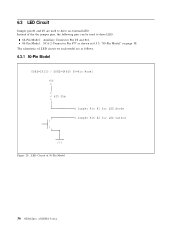
LED Circuit 34 OEM Spec. 6.2.1.9 Disable SCSI Parity Check (Position 11) Grounding this pin will disable SCSI Parity checking. 6.2.1.10 LED pins (Position 12) The LED pins are used to 30 mA of sink current capability is then connected to the Pin #2 to the current limited + 5 V source provided on Pin #1 of DDRS-3xxxx Up to drive an external Light Emitting Diode. The LED Cathode is provided. of the Option Jumper Block. The LED Anode must be tied to complete the circuit. +5V o > < 620 Ohm > / \ o Pin #1 for LED Anode o Pin #2 for LED Cathod /// Figure 25.
LED Circuit 34 OEM Spec. 6.2.1.9 Disable SCSI Parity Check (Position 11) Grounding this pin will disable SCSI Parity checking. 6.2.1.10 LED pins (Position 12) The LED pins are used to 30 mA of sink current capability is then connected to the Pin #2 to the current limited + 5 V source provided on Pin #1 of DDRS-3xxxx Up to drive an external Light Emitting Diode. The LED Cathode is provided. of the Option Jumper Block. The LED Anode must be tied to complete the circuit. +5V o > < 620 Ohm > / \ o Pin #1 for LED Anode o Pin #2 for LED Cathod /// Figure 25.
Hard Drive Specifications
Page 46
of 50-Pin Model 36 OEM Spec. 6.3 LED Circuit Jumper pin #1 and #2 are as follows. 6.3.1 50-Pin Model DDRS 39130 / DDRS 34560 50 Pin Model +5V o > < 620 Ohm > o Jumper Pin #1 for LED Anode o Jumper Pin #2 for LED Cathod / \ /// Figure 28. Instead of LED circuit on page 38. LED Circuit of DDRS-3xxxx The schematics of the the jumper pins, the following pins can be used to drive LED. 68-Pin Model : Auxiliary Connector Pin #8 and #11. 80-Pin Model : SCA-2 Connector Pin #77 as shown in 6.3.3, "80-Pin Model" on each model are used to drive an external LED.
of 50-Pin Model 36 OEM Spec. 6.3 LED Circuit Jumper pin #1 and #2 are as follows. 6.3.1 50-Pin Model DDRS 39130 / DDRS 34560 50 Pin Model +5V o > < 620 Ohm > o Jumper Pin #1 for LED Anode o Jumper Pin #2 for LED Cathod / \ /// Figure 28. Instead of LED circuit on page 38. LED Circuit of DDRS-3xxxx The schematics of the the jumper pins, the following pins can be used to drive LED. 68-Pin Model : Auxiliary Connector Pin #8 and #11. 80-Pin Model : SCA-2 Connector Pin #77 as shown in 6.3.3, "80-Pin Model" on each model are used to drive an external LED.
Hard Drive Specifications
Page 48
of 80-Pin (SCA-2) Model 38 OEM Spec. LED Circuit of DDRS-3xxxx 6.3.3 80-Pin Model DDRS 39130 / DDRS 34560 80 Pin (SCA 2) Model : : : : +5V +5V : o o : : : > > : 1K Ohm < < 620 Ohm : > > : : : : \/ : LED \ / : Jumper Pin #1 for LED Anode o : : : o / Jumper Pin #2 for LED Cathod \ : : : SCA 2 Connector Pin #77 /// o for LED Cathod : : : Example of Usage : at System Side : : : +5V : o : : : > : < 150 Ohm : > : : : : \/ : \ / LED : : : : : : : : : : : : : o : : : Figure 30.
of 80-Pin (SCA-2) Model 38 OEM Spec. LED Circuit of DDRS-3xxxx 6.3.3 80-Pin Model DDRS 39130 / DDRS 34560 80 Pin (SCA 2) Model : : : : +5V +5V : o o : : : > > : 1K Ohm < < 620 Ohm : > > : : : : \/ : LED \ / : Jumper Pin #1 for LED Anode o : : : o / Jumper Pin #2 for LED Cathod \ : : : SCA 2 Connector Pin #77 /// o for LED Cathod : : : Example of Usage : at System Side : : : +5V : o : : : > : < 150 Ohm : > : : : : \/ : \ / LED : : : : : : : : : : : : : o : : : Figure 30.

Hard Drive Specifications
Page 50
... temperature as shown below 60˚ C at the center of the top cover of DDRS-3xxxx of the drive. The system has to provide sufficient ventilation to maintain a surface temperature below . Maximum ...Allowable Module Surface Temperature Module Name Location Maximum Allowable Surface Temperature MPU + HDC 1 85˚ C DRAM 2 90˚ C SCSI Terminator 3 90˚ C VCM + Spindle Driver 4 90˚ C Cannel 5 90˚ C Figure 33. Module Location 40 OEM Spec...
... temperature as shown below 60˚ C at the center of the top cover of DDRS-3xxxx of the drive. The system has to provide sufficient ventilation to maintain a surface temperature below . Maximum ...Allowable Module Surface Temperature Module Name Location Maximum Allowable Surface Temperature MPU + HDC 1 85˚ C DRAM 2 90˚ C SCSI Terminator 3 90˚ C VCM + Spindle Driver 4 90˚ C Cannel 5 90˚ C Figure 33. Module Location 40 OEM Spec...

Hard Drive Specifications
Page 52
...37. Power Supply Generated Ripple at Drive Power Connector Maximum +5V DC 100 [ mV pp] +12V DC 150 [ mV pp] Notes 0-10 [MHz] 0-10 [MHz] During drive start up and seeking, 12 volt ripple is a more desirable method of DDRS-34560 42 OEM Spec. To prevent external electrical noise from... interfering with separate power leads to each drive is generated by four screws in a user system frame which has...
...37. Power Supply Generated Ripple at Drive Power Connector Maximum +5V DC 100 [ mV pp] +12V DC 150 [ mV pp] Notes 0-10 [MHz] 0-10 [MHz] During drive start up and seeking, 12 volt ripple is a more desirable method of DDRS-34560 42 OEM Spec. To prevent external electrical noise from... interfering with separate power leads to each drive is generated by four screws in a user system frame which has...

Hard Drive Specifications
Page 54
6.7.6 Automatic Drive Maintenance (ADM) A D M function can be enabled by EADM bit in Mode Page 0, and the shipping default is to enhance the reliability in 10.19.1.1, "Automatic Drive Maintenance (ADM)" on page 197. 6.7.7 Preventive Maintenance None. 44 OEM Spec. The details are described in continuous usage. A D M function is equipped to perform a CSS automatically after detection of idling time for 1 minute at intervals of DDRS-3xxxx A D M function is disable. of 1 week.
6.7.6 Automatic Drive Maintenance (ADM) A D M function can be enabled by EADM bit in Mode Page 0, and the shipping default is to enhance the reliability in 10.19.1.1, "Automatic Drive Maintenance (ADM)" on page 197. 6.7.7 Preventive Maintenance None. 44 OEM Spec. The details are described in continuous usage. A D M function is equipped to perform a CSS automatically after detection of idling time for 1 minute at intervals of DDRS-3xxxx A D M function is disable. of 1 week.

Hard Drive Specifications
Page 56
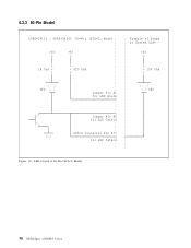
of 68-pin Model 46 OEM Spec. 6.8.1.2 68-pin Model Figure 40. Outline of DDRS-3xxxx
of 68-pin Model 46 OEM Spec. 6.8.1.2 68-pin Model Figure 40. Outline of DDRS-3xxxx