
User Manual
Page 7
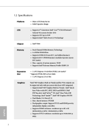
...• Supports Intel® Turbo Boost 2.0 Technology Chipset • Intel® H110 Memory • Dual Channel DDR4 Memory Technology • 2 x DDR4 DIMM Slots • Supports DDR4 2133 non-ECC, un-buffered memory • Supports ECC UDIMM memory modules (operate in Visuals : Intel® Quick...; Supports DVI-D with AVC, MVC (S3D) and MPEG-2 Full HW Encode1, Intel® InTruTM 3D, Intel® Clear Video HD Technology, Intel® InsiderTM, Intel® HD Graphics 510/530 • Pixel Shader 5.0, DirectX 12 • Max. ECC mode) • Max. capacity of system memory: 32GB...
...• Supports Intel® Turbo Boost 2.0 Technology Chipset • Intel® H110 Memory • Dual Channel DDR4 Memory Technology • 2 x DDR4 DIMM Slots • Supports DDR4 2133 non-ECC, un-buffered memory • Supports ECC UDIMM memory modules (operate in Visuals : Intel® Quick...; Supports DVI-D with AVC, MVC (S3D) and MPEG-2 Full HW Encode1, Intel® InTruTM 3D, Intel® Clear Video HD Technology, Intel® InsiderTM, Intel® HD Graphics 510/530 • Pixel Shader 5.0, DirectX 12 • Max. ECC mode) • Max. capacity of system memory: 32GB...
User Manual
Page 12
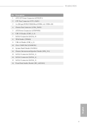
Description 1 ATX 12V Power Connector (ATX12V1) 2 CPU Fan Connector (CPU_FAN1) 3 2 x 288-pin DDR4 DIMM Slots (DDR4_A1, DDR4_B1) 4 Chassis Fan Connector (CHA_FAN1) 5 ATX Power Connector (ATXPWR1) 6 USB 3.0 Header (USB3_3_4) 7 SATA3 Connector (SATA3_0) 8 TPM Header (TPMS1) 9 USB 2.0 Header (USB_4_5) 10 Clear CMOS Pad (CLRMOS1) 11 System Panel Header (PANEL1) 12 Chassis Intrusion and Speaker Header (SPK_CI1) 13 SATA3 Connector (SATA3_1) 14 SATA3 Connector (SATA3_2) 15 SATA3 Connector (SATA3_3) 16 Front Panel Audio Header (HD_AUDIO1) H110M-HDS English 7 No.
Description 1 ATX 12V Power Connector (ATX12V1) 2 CPU Fan Connector (CPU_FAN1) 3 2 x 288-pin DDR4 DIMM Slots (DDR4_A1, DDR4_B1) 4 Chassis Fan Connector (CHA_FAN1) 5 ATX Power Connector (ATXPWR1) 6 USB 3.0 Header (USB3_3_4) 7 SATA3 Connector (SATA3_0) 8 TPM Header (TPMS1) 9 USB 2.0 Header (USB_4_5) 10 Clear CMOS Pad (CLRMOS1) 11 System Panel Header (PANEL1) 12 Chassis Intrusion and Speaker Header (SPK_CI1) 13 SATA3 Connector (SATA3_1) 14 SATA3 Connector (SATA3_2) 15 SATA3 Connector (SATA3_3) 16 Front Panel Audio Header (HD_AUDIO1) H110M-HDS English 7 No.
User Manual
Page 20
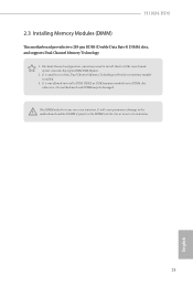
... DIMM may be damaged.. It will cause permanent damage to activate Dual Channel Memory Technology with only one correct orientation. H110M-HDS 2.3 Installing Memory Modules (DIMM) This motherboard provides two 288-pin DDR4 (Double Data Rate 4) DIMM slots, and supports Dual Channel Memory Technology. 1. It is not allowed to install identical (the same...
... DIMM may be damaged.. It will cause permanent damage to activate Dual Channel Memory Technology with only one correct orientation. H110M-HDS 2.3 Installing Memory Modules (DIMM) This motherboard provides two 288-pin DDR4 (Double Data Rate 4) DIMM slots, and supports Dual Channel Memory Technology. 1. It is not allowed to install identical (the same...
User Manual
Page 43
... a column address to the memory and the beginning of the data in watts. RAS# to CAS# Delay and Row Precharge (tRCDtRP) O RAS# to overclock the DDR4 memory and perform beyond standard specifications. DRAM Reference Clock Select Auto for optimized settings. Primary Timing CAS# Latency (tCL) The time between a bank active command...
... a column address to the memory and the beginning of the data in watts. RAS# to CAS# Delay and Row Precharge (tRCDtRP) O RAS# to overclock the DDR4 memory and perform beyond standard specifications. DRAM Reference Clock Select Auto for optimized settings. Primary Timing CAS# Latency (tCL) The time between a bank active command...
User Manual
Page 44
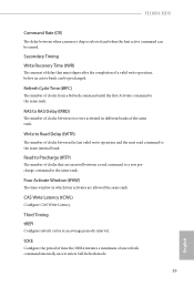
...The time window in different banks of a valid write operation, before an active bank can be precharged. tCKE Configure the period of time the DDR4 initiates a minimum of clocks from a Refresh command until the first Activate command to the same internal bank. Write to the same rank. Secondary... read command to the same rank. Read to Precharge (tRTP) The number of clocks that must elapse after the completion of the same rank. H110M-HDS Command Rate (CR) The delay between when a memory chip is selected and when the first active command can be issued. Refresh Cycle Time (...
...The time window in different banks of a valid write operation, before an active bank can be precharged. tCKE Configure the period of time the DDR4 initiates a minimum of clocks from a Refresh command until the first Activate command to the same internal bank. Write to the same rank. Secondary... read command to the same rank. Read to Precharge (tRTP) The number of clocks that must elapse after the completion of the same rank. H110M-HDS Command Rate (CR) The delay between when a memory chip is selected and when the first active command can be issued. Refresh Cycle Time (...