Service Manual
Page 1
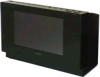
... mm Mass (excl. HCD-SLK1i/SLK2i SERVICE MANUAL Ver. 1.0 2010.06 Photo: HCD-SLK1i • HCD-SLK1i is the amplifier, USB, memory card, disc player and tuner section in WHG-SLK1i. • HCD-SLK2i is the value measurement at 8 Ω, 1 kHz) SPECIFICATIONS Inputs VIDEO/SAT VIDEO IN: 1 Vp-p, 75 Ω VIDEO/SAT AUDIO IN: voltage 250/450 mV, impedance 47 kΩ Outputs DVD VIDEO OUT: max. rated 35 watts per channel at a distance...
... mm Mass (excl. HCD-SLK1i/SLK2i SERVICE MANUAL Ver. 1.0 2010.06 Photo: HCD-SLK1i • HCD-SLK1i is the amplifier, USB, memory card, disc player and tuner section in WHG-SLK1i. • HCD-SLK2i is the value measurement at 8 Ω, 1 kHz) SPECIFICATIONS Inputs VIDEO/SAT VIDEO IN: 1 Vp-p, 75 Ω VIDEO/SAT AUDIO IN: voltage 250/450 mV, impedance 47 kΩ Outputs DVD VIDEO OUT: max. rated 35 watts per channel at a distance...

Service Manual
Page 2
... Precision 245 digital multimeter is suitable for AC leakage. A) To Exposed Metal Parts on the rear exterior. REPLACE THESE COMPONENTS WITH SONY PARTS WHOSE PART NUMBERS APPEAR AS SHOWN IN THIS MANUAL OR IN SUPPLEMENTS PUBLISHED BY SONY. ATTENTION AU COMPOSANT AYANT RAPPORT À LA SÉCURITÉ! SDHC Logo is protected by the developer to chassis, must have a 2 V AC range are used under...
... Precision 245 digital multimeter is suitable for AC leakage. A) To Exposed Metal Parts on the rear exterior. REPLACE THESE COMPONENTS WITH SONY PARTS WHOSE PART NUMBERS APPEAR AS SHOWN IN THIS MANUAL OR IN SUPPLEMENTS PUBLISHED BY SONY. ATTENTION AU COMPOSANT AYANT RAPPORT À LA SÉCURITÉ! SDHC Logo is protected by the developer to chassis, must have a 2 V AC range are used under...

Service Manual
Page 3
...-12. 3 SERVICING NOTES 4 2. Rear Case Block 10 2-4. Belt (MOT 15 2-12. AUDIO OUTPUT Section 23 4-4. VIDEO Section 24 4-5. DISPLAY Section (1/7 27 4-7. DISPLAY Section (3/7 29 4-9. Schematic Diagram - Printed Wiring Board - MAIN Board (3/4 48 4-28. MAIN Board Section 66 5-4. HCD-SLK1i/SLK2i TABLE OF CONTENTS 1. DISASSEMBLY 2-1. Switching Regulator Block 12 2-7. LCD Board 16 2-13. Block Diagram - PANEL, POWER SUPPLY Section 25 4-6. Schematic Diagram - DISPLAY Section (4/7 30 4-10. DISPLAY Section (6/7 32 4-12. DISPLAY Section...
...-12. 3 SERVICING NOTES 4 2. Rear Case Block 10 2-4. Belt (MOT 15 2-12. AUDIO OUTPUT Section 23 4-4. VIDEO Section 24 4-5. DISPLAY Section (1/7 27 4-7. DISPLAY Section (3/7 29 4-9. Schematic Diagram - Printed Wiring Board - MAIN Board (3/4 48 4-28. MAIN Board Section 66 5-4. HCD-SLK1i/SLK2i TABLE OF CONTENTS 1. DISASSEMBLY 2-1. Switching Regulator Block 12 2-7. LCD Board 16 2-13. Block Diagram - PANEL, POWER SUPPLY Section 25 4-6. Schematic Diagram - DISPLAY Section (4/7 30 4-10. DISPLAY Section (6/7 32 4-12. DISPLAY Section...

Service Manual
Page 4
... the disc reflective surface by the charged electrostatic load, etc. HCD-SLK1i/SLK2i SECTION 1 SERVICING NOTES NOTES ON HANDLING THE OPTICAL PICK-UP BLOCK OR BASE UNIT The laser diode in the optical pick-up block may suffer electrostatic break-down and also use the procedure in the printed matter which is included in the repair parts...
... the disc reflective surface by the charged electrostatic load, etc. HCD-SLK1i/SLK2i SECTION 1 SERVICING NOTES NOTES ON HANDLING THE OPTICAL PICK-UP BLOCK OR BASE UNIT The laser diode in the optical pick-up block may suffer electrostatic break-down and also use the procedure in the printed matter which is included in the repair parts...

Service Manual
Page 6
disc - IP BOARD SERVICE POSITION Note: Neither the wire from switching regulator fan cable DISPLAY board IP board 6 Please rotate the pully in the direction of the arrow after removing mechanism deck, and eject the disc. DVD mechanism block bottom view - fan motor wire from switching regulator nor the fan cable must loosen. HCD-SLK1i/SLK2i HOW TO EJECT THE DISC WHEN POWER SWITCH TURNS OFF Note: Please take out the DVD mechanism block from a set referring to "SECTION 2 DISASSEMBLY".
disc - IP BOARD SERVICE POSITION Note: Neither the wire from switching regulator fan cable DISPLAY board IP board 6 Please rotate the pully in the direction of the arrow after removing mechanism deck, and eject the disc. DVD mechanism block bottom view - fan motor wire from switching regulator nor the fan cable must loosen. HCD-SLK1i/SLK2i HOW TO EJECT THE DISC WHEN POWER SWITCH TURNS OFF Note: Please take out the DVD mechanism block from a set referring to "SECTION 2 DISASSEMBLY".

Service Manual
Page 7
... thirteen pins. Jig No. MAIN BOARD SERVICE POSITION • Please connect following extension jig. Connect extension jig 1 to the MAIN board (CN301) and DISPLAY board (CN302) HCD-SLK1i/SLK2i CN302 CN408 DISPLAY board Connect extension jig 1 to the MAIN board (CN101) and DISPLAY board (CN408) CN101 CN301 MAIN board TERMINAL board SWITCHING REGULATOR 7 Jig No. Part No. Pitch (mm) Cores Length...
... thirteen pins. Jig No. MAIN BOARD SERVICE POSITION • Please connect following extension jig. Connect extension jig 1 to the MAIN board (CN301) and DISPLAY board (CN302) HCD-SLK1i/SLK2i CN302 CN408 DISPLAY board Connect extension jig 1 to the MAIN board (CN101) and DISPLAY board (CN408) CN101 CN301 MAIN board TERMINAL board SWITCHING REGULATOR 7 Jig No. Part No. Pitch (mm) Cores Length...

Service Manual
Page 17
SECTION 3 TEST MODE HCD-SLK1i/SLK2i COLD RESET Reset the system to turn on the system. 2. Touch the [M], [m], [ Press the [?/1] button to its factory default settings. Procedure: 1.
SECTION 3 TEST MODE HCD-SLK1i/SLK2i COLD RESET Reset the system to turn on the system. 2. Touch the [M], [m], [ Press the [?/1] button to its factory default settings. Procedure: 1.

Service Manual
Page 18
Press the [?/1] button to take sample disc out of disc slot in the shop. Touch the [M], [m], [ Procedure: 1. Touch the [HOME] sensor. 3. HCD-SLK1i/SLK2i DISC ANTITHEFT LOCK This mode is used to unable to turn on the system. 2.
Press the [?/1] button to take sample disc out of disc slot in the shop. Touch the [M], [m], [ Procedure: 1. Touch the [HOME] sensor. 3. HCD-SLK1i/SLK2i DISC ANTITHEFT LOCK This mode is used to unable to turn on the system. 2.

Service Manual
Page 19
... Gain Adjust: 5. Iop: 7. Level: 8. IOP" by pressing the [2] button on the remote commander. Manual Adjust 1. Level: 8. S curve(FE) Level: 9. Please find the label on the rear of emergency history, press [.] or [>] button on the remote commander. Emg. You can check the total time when the laser is OK. The error code consists of Remocon Diagnosis Menu, select "3. Servo Control 2. The screen will appear as shown. Focus Balance Adjust: 4. MIRR Time: [ M ] [ m ] Change...
... Gain Adjust: 5. Iop: 7. Level: 8. IOP" by pressing the [2] button on the remote commander. Manual Adjust 1. Level: 8. S curve(FE) Level: 9. Please find the label on the rear of emergency history, press [.] or [>] button on the remote commander. Emg. You can check the total time when the laser is OK. The error code consists of Remocon Diagnosis Menu, select "3. Servo Control 2. The screen will appear as shown. Focus Balance Adjust: 4. MIRR Time: [ M ] [ m ] Change...

Service Manual
Page 20
... Setup Data Press [DVD MENU] button and then press [CLEAR] button on the remote commander. x.xxx Firm (Sub) : xx.xx RISC : xxxxxx 8032 : xxxxxx Audio DSP : xx.xx.xx.xx Servo DSP : xx.xx.xx.xx [0] Return to Top Menu To return to the Top Menu of Remocon Diagnosis Menu, press [0] button on -screen display. Clear the Laser Hour Press [ DISPLAY] button and then press [CLEAR] button on the remote...
... Setup Data Press [DVD MENU] button and then press [CLEAR] button on the remote commander. x.xxx Firm (Sub) : xx.xx RISC : xxxxxx 8032 : xxxxxx Audio DSP : xx.xx.xx.xx Servo DSP : xx.xx.xx.xx [0] Return to Top Menu To return to the Top Menu of Remocon Diagnosis Menu, press [0] button on -screen display. Clear the Laser Hour Press [ DISPLAY] button and then press [CLEAR] button on the remote...

Service Manual
Page 21
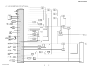
...AUTO POWER CONTROL (FOR CD) Q003 (1/2) REG02 AUTO POWER CONTROL (FOR DVD) Q003 (2/2) 17 LDO1 18 LDO2 RF AMP, SERVO DSP, DVD/CD DECODER IC005 MSW VR (780) VR (650) CD ON SWITCH Q001 (1/2) DVD ON SWITCH Q001 (2/2) Q002 VCC FCS+ FCSTRK+ TRK- RA11 RD0 - SIGNAL PATH : DISC PLAY : VIDEO...UDQM FLASH ROM IC003 1 _CS 2 SO 5 SI 6 SCK R-ch is omitted due to same as L-ch. SL- BLOCK DIAGRAM ...HCD-SLK1i/SLK2i 25 LOADING 16 24 MOTOR DRIVE 17 44 REV 45 FWD 43 OCSW1 42 CKSW1 6 TRG-SW DVD_XIFBUSY XIFCS DVD_SOD DVD_SID DVD_SCO XSYSRST 25 27 24 22 23 21 SYSTEM CONTROLLER IC100 (1/3) AML RESET...
...AUTO POWER CONTROL (FOR CD) Q003 (1/2) REG02 AUTO POWER CONTROL (FOR DVD) Q003 (2/2) 17 LDO1 18 LDO2 RF AMP, SERVO DSP, DVD/CD DECODER IC005 MSW VR (780) VR (650) CD ON SWITCH Q001 (1/2) DVD ON SWITCH Q001 (2/2) Q002 VCC FCS+ FCSTRK+ TRK- RA11 RD0 - SIGNAL PATH : DISC PLAY : VIDEO...UDQM FLASH ROM IC003 1 _CS 2 SO 5 SI 6 SCK R-ch is omitted due to same as L-ch. SL- BLOCK DIAGRAM ...HCD-SLK1i/SLK2i 25 LOADING 16 24 MOTOR DRIVE 17 44 REV 45 FWD 43 OCSW1 42 CKSW1 6 TRG-SW DVD_XIFBUSY XIFCS DVD_SOD DVD_SID DVD_SCO XSYSRST 25 27 24 22 23 21 SYSTEM CONTROLLER IC100 (1/3) AML RESET...
Service Manual
Page 25
... LED DRIVE Q264 USB POWER 66 87 TIMER LED D266 AUTO STANDBY D901, 902 (SONY LOGO) LED DRIVE Q265 LED DRIVE Q901 AMBIENT LIGHT SENSOR PHOTO DIODE PH901 88 A. 4-5. CONT 60 PROTECT-INT 19 D200 EVER+3.3V AD-LINE_PULL-UP B+ SWITCH Q198, 199 RESET SWITCH Q202 RESET SIGNAL GENERATOR Q201 +4V REGULATOR IC908 D909 B+ SWITCH Q905 - 907 D908 HCD-SLK1i/SLK2i 25 25 +9V...
... LED DRIVE Q264 USB POWER 66 87 TIMER LED D266 AUTO STANDBY D901, 902 (SONY LOGO) LED DRIVE Q265 LED DRIVE Q901 AMBIENT LIGHT SENSOR PHOTO DIODE PH901 88 A. 4-5. CONT 60 PROTECT-INT 19 D200 EVER+3.3V AD-LINE_PULL-UP B+ SWITCH Q198, 199 RESET SWITCH Q202 RESET SIGNAL GENERATOR Q201 +4V REGULATOR IC908 D909 B+ SWITCH Q905 - 907 D908 HCD-SLK1i/SLK2i 25 25 +9V...

Service Manual
Page 26
... numbers refer to this diagrams. • Indication of conventional IC CSP (Chip Size Package) • Circuit Boards Location KEY-LEFT board DISPLAY board HP board IP board MAIN board KEY-RIGHT board TUNER (FM/AM) MS-214 board LCD board SWITCHING REGULATOR TOUCH PANEL board TERMINAL board JACK board HCD-SLK1i/SLK2i 26 26 Lead layout of transistor. Parts face...
... numbers refer to this diagrams. • Indication of conventional IC CSP (Chip Size Package) • Circuit Boards Location KEY-LEFT board DISPLAY board HP board IP board MAIN board KEY-RIGHT board TUNER (FM/AM) MS-214 board LCD board SWITCHING REGULATOR TOUCH PANEL board TERMINAL board JACK board HCD-SLK1i/SLK2i 26 26 Lead layout of transistor. Parts face...
Service Manual
Page 39
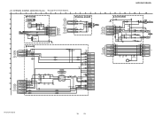
SCHEMATIC DIAGRAM - TB601 SPEAKERS F DISPLAY BOARD (3/7) CN604 (Page 29) C1012 100 16V C1016 0.1 IC B/D IC1001 VIDEO AMP IC1001 NJM2505AF(TE2) 5 3 V+ 1.7 VIN 4 2 GND 1 1.7 1 VOUT VGND 5 CL1004 R1004 0 C1009 10 C1006 10 R1003 75 R1009 1k R1007 100 CN1003 30P (iPod Dock)... 2 1 GND RESET CN_VSS RXD1 CLK1 MCU_VCC RTS1 TXD1 DGND (NC) BZ701 HCD-SLK1i/SLK2i 39 39 HCD-SLK1i/SLK2i 4-18. AUDIO IN/OUT Section - • See page 50 for IC Block Diagrams. 1 2 3 4 5 6 7 8 9 10 11 12 13 14 HP BOARD A IC242 REMOTE CONTROL RECEIVER IC242 PNA4823M05S0 R241 ...
SCHEMATIC DIAGRAM - TB601 SPEAKERS F DISPLAY BOARD (3/7) CN604 (Page 29) C1012 100 16V C1016 0.1 IC B/D IC1001 VIDEO AMP IC1001 NJM2505AF(TE2) 5 3 V+ 1.7 VIN 4 2 GND 1 1.7 1 VOUT VGND 5 CL1004 R1004 0 C1009 10 C1006 10 R1003 75 R1009 1k R1007 100 CN1003 30P (iPod Dock)... 2 1 GND RESET CN_VSS RXD1 CLK1 MCU_VCC RTS1 TXD1 DGND (NC) BZ701 HCD-SLK1i/SLK2i 39 39 HCD-SLK1i/SLK2i 4-18. AUDIO IN/OUT Section - • See page 50 for IC Block Diagrams. 1 2 3 4 5 6 7 8 9 10 11 12 13 14 HP BOARD A IC242 REMOTE CONTROL RECEIVER IC242 PNA4823M05S0 R241 ...

Service Manual
Page 48
... TIMER LED 0 88 A.STBY LED 0 89 PLAY LED 0 90 PAUSE LED JL231 91 NO USE 0 92 VACS JL233 93 NO USE 3.3 94 LUX-SENSOR 0 95 DEST-IN 96 AVSS 0 97 3.5 98 3.5 99 3.5 100 DSP-RESET DVD 3.3V MONITOR AD-KEY-2 MODEL VREF AVCC AD-SWITCH IC100 SYSTEM CONTROLLER IC100 R5F364AMDFA PROTECT AMP /OTW2 /OTW1 /D-AMP-RESET 3.7 EEPROM-CLK 50 3.7 EEPROM-DATA 49 3.3 TP SCL...
... TIMER LED 0 88 A.STBY LED 0 89 PLAY LED 0 90 PAUSE LED JL231 91 NO USE 0 92 VACS JL233 93 NO USE 3.3 94 LUX-SENSOR 0 95 DEST-IN 96 AVSS 0 97 3.5 98 3.5 99 3.5 100 DSP-RESET DVD 3.3V MONITOR AD-KEY-2 MODEL VREF AVCC AD-SWITCH IC100 SYSTEM CONTROLLER IC100 R5F364AMDFA PROTECT AMP /OTW2 /OTW1 /D-AMP-RESET 3.7 EEPROM-CLK 50 3.7 EEPROM-DATA 49 3.3 TP SCL...

Service Manual
Page 55
...) output terminal I Current reference input terminal Fixed at "L" in this set I Laser power monitor input from the optical pick-up block O Laser diode drive signal output to the SD-RAM - Power supply terminal (+3.3V) I /O USB generating reference current input/output terminal - HCD-SLK1i/SLK2i • IC Pin Function Description DISPLAY BOARD IC005 (RF AMP, SERVO DSP, DVD/CD DECODER) CXD9970R (LE) (SLK1i: US and Canadian models)/CXD9971R (LE) (Except SLK1i: US and Canadian models...
...) output terminal I Current reference input terminal Fixed at "L" in this set I Laser power monitor input from the optical pick-up block O Laser diode drive signal output to the SD-RAM - Power supply terminal (+3.3V) I /O USB generating reference current input/output terminal - HCD-SLK1i/SLK2i • IC Pin Function Description DISPLAY BOARD IC005 (RF AMP, SERVO DSP, DVD/CD DECODER) CXD9970R (LE) (SLK1i: US and Canadian models)/CXD9971R (LE) (Except SLK1i: US and Canadian models...

Service Manual
Page 60
... I Protect signal input terminal I Ready signal input from the digital power amplifier I Clipping warning signal input from the digital power amplifier I VBUS over current detection signal input terminal for USB connector I VBUS over current detection signal input terminal for D/A converter Not used I Fixed at "H" in this set I Chucking detection switch input terminal I Main system clock (5 MHz) input terminal - after the power supply rises, "L" is connected O Buzzer level control signal output terminal I SIRCS signal input from remote control receiver O Reset...
... I Protect signal input terminal I Ready signal input from the digital power amplifier I Clipping warning signal input from the digital power amplifier I VBUS over current detection signal input terminal for USB connector I VBUS over current detection signal input terminal for D/A converter Not used I Fixed at "H" in this set I Chucking detection switch input terminal I Main system clock (5 MHz) input terminal - after the power supply rises, "L" is connected O Buzzer level control signal output terminal I SIRCS signal input from remote control receiver O Reset...

Service Manual
Page 61
... I Model setting terminal I /O Description O LED drive signal output terminal for ON/STANDBY indicator "L": red LED on (STANDBY), "H": green LED on (ON) O Power on/off control signal output terminal for pull-up of A/D input line "H": power on O Not used I VACS signal input from the digital audio processor O Not used I Ambient light sensor input terminal I Protect signal input from the digital audio processor O Muting on/off control signal output to the digital audio processor "L": muting on O Reset signal output to the digital audio processor "L": reset I Power (DVD +3.3V) monitor...
... I Model setting terminal I /O Description O LED drive signal output terminal for ON/STANDBY indicator "L": red LED on (STANDBY), "H": green LED on (ON) O Power on/off control signal output terminal for pull-up of A/D input line "H": power on O Not used I VACS signal input from the digital audio processor O Not used I Ambient light sensor input terminal I Protect signal input from the digital audio processor O Muting on/off control signal output to the digital audio processor "L": muting on O Reset signal output to the digital audio processor "L": reset I Power (DVD +3.3V) monitor...

Service Manual
Page 62
... - Power supply terminal (+3.3V) Not used PWM2_RD, PWM2_RI O Digital audio signal output terminal Not used PWM3_LD, PWM3_LI O Digital audio (R-ch) signal output to the system controller DVDD2 - Ground terminal VR_DIG2 - Ground terminal XVREG_EN I Voltage regulator enable signal input terminal "L": regulator on /RESET I Reset signal input from the system controller "L": muting on Fixed at "L" in this set STEST I Test terminal MCLKOUT O Master clock signal output terminal Not used LRCLKOUT O L/R sampling clock signal output terminal Not used SCLKOUT O Bit clock signal...
... - Power supply terminal (+3.3V) Not used PWM2_RD, PWM2_RI O Digital audio signal output terminal Not used PWM3_LD, PWM3_LI O Digital audio (R-ch) signal output to the system controller DVDD2 - Ground terminal VR_DIG2 - Ground terminal XVREG_EN I Voltage regulator enable signal input terminal "L": regulator on /RESET I Reset signal input from the system controller "L": muting on Fixed at "L" in this set STEST I Test terminal MCLKOUT O Master clock signal output terminal Not used LRCLKOUT O L/R sampling clock signal output terminal Not used SCLKOUT O Bit clock signal...

Service Manual
Page 63
... input from the AUDIO IN jack - Power supply terminal (+3.3V) O Analog audio (L-ch) signal (for VACS signal) output to the system controller - PLL filter terminal - External capacitor connection terminal for VACS signal) output to the system controller O Analog audio (R-ch) signal (for internal +1.8V regulator - Power supply terminal (+3.3V) - Ground terminal 63 Power supply terminal (+3.3V) O Digital audio (L-ch) signal output terminal for headphone O Digital audio (L-ch) signal output terminal for headphone O Digital audio (L-ch) signal output terminal Not used...
... input from the AUDIO IN jack - Power supply terminal (+3.3V) O Analog audio (L-ch) signal (for VACS signal) output to the system controller - PLL filter terminal - External capacitor connection terminal for VACS signal) output to the system controller O Analog audio (R-ch) signal (for internal +1.8V regulator - Power supply terminal (+3.3V) - Ground terminal 63 Power supply terminal (+3.3V) O Digital audio (L-ch) signal output terminal for headphone O Digital audio (L-ch) signal output terminal for headphone O Digital audio (L-ch) signal output terminal Not used...

