Service Manual
Page 2
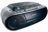
...heat. on the conductor when soldering or unsoldering. COMPONENTS IDENTIFIED BY MARK 0 OR DOTTED LINE WITH MARK 0 ON THE SCHEMATIC DIAGRAMS AND IN THE PARTS LIST ARE CRITICAL TO SAFE OPERATION. Notes on this model is concentrated so as to electrostatic breakdown... (EXCEPT CND, E92, MX model) Battery life For CD radio cassette-corder: FM recording Sony R14P: approx. 6 h Sony alkaline LR14: approx. 20 h Tape playback Sony R14P: approx. 3 h Sony alkaline LR14: approx. 12 h CD playback Sony R14P: approx. 1.5 h Sony alkaline LR14: approx. 4.5 h Dimensions Approx. 360 × 141 × 235 mm ...
...heat. on the conductor when soldering or unsoldering. COMPONENTS IDENTIFIED BY MARK 0 OR DOTTED LINE WITH MARK 0 ON THE SCHEMATIC DIAGRAMS AND IN THE PARTS LIST ARE CRITICAL TO SAFE OPERATION. Notes on this model is concentrated so as to electrostatic breakdown... (EXCEPT CND, E92, MX model) Battery life For CD radio cassette-corder: FM recording Sony R14P: approx. 6 h Sony alkaline LR14: approx. 20 h Tape playback Sony R14P: approx. 3 h Sony alkaline LR14: approx. 12 h CD playback Sony R14P: approx. 1.5 h Sony alkaline LR14: approx. 4.5 h Dimensions Approx. 360 × 141 × 235 mm ...
Service Manual
Page 3
... the heated tip is applied for a slightly longer time. DISASSEMBLY 3-1. Power Board 12 4. MECHANICAL ADJUSTMENTS 13 5. DIAGRAMS 6-1. Schematic Diagram - Printed Wiring Boards - Schematic Diagram - Power Supply Section 30 6-15. Cabinet (Front) Assy, Cabinet (Upper) Assy 7 3-3. Optical Pick-up 9.... • Unleaded solder melts at a temperature about 350°C. Main Board 8 3-4. CD Lid 10 3-9. Schematic Diagram - Schematic Diagram - TABLE OF CONTENTS 1. Block Diagram - Power Supply Section 31 7. Rear Cabinet Section 39 7-2. Main Section (1/3 23...
... the heated tip is applied for a slightly longer time. DISASSEMBLY 3-1. Power Board 12 4. MECHANICAL ADJUSTMENTS 13 5. DIAGRAMS 6-1. Schematic Diagram - Printed Wiring Boards - Schematic Diagram - Power Supply Section 30 6-15. Cabinet (Front) Assy, Cabinet (Upper) Assy 7 3-3. Optical Pick-up 9.... • Unleaded solder melts at a temperature about 350°C. Main Board 8 3-4. CD Lid 10 3-9. Schematic Diagram - Schematic Diagram - TABLE OF CONTENTS 1. Block Diagram - Power Supply Section 31 7. Rear Cabinet Section 39 7-2. Main Section (1/3 23...

Service Manual
Page 19
CIRCUIT BOARDS LOCATION HEADPHONE board POWER board BD83S board BATTERY-1 board KEY-1 board PANEL board MAIN board TC board BATTERY-2 board KEY-2 board • Waveforms - CET : East European & Russian model. KR : Korea model MX : Mexican model. TH : Thai model. SP : Singapore model. Voltage variations may be noted due to normal production tolerances. • Circled numbers refer to normal production tolerances. • Waveforms are taken with part number. • f : internal component. • : Pattern from the side which enables seeing. (The other ...
CIRCUIT BOARDS LOCATION HEADPHONE board POWER board BD83S board BATTERY-1 board KEY-1 board PANEL board MAIN board TC board BATTERY-2 board KEY-2 board • Waveforms - CET : East European & Russian model. KR : Korea model MX : Mexican model. TH : Thai model. SP : Singapore model. Voltage variations may be noted due to normal production tolerances. • Circled numbers refer to normal production tolerances. • Waveforms are taken with part number. • f : internal component. • : Pattern from the side which enables seeing. (The other ...

Service Manual
Page 21
... to page 19 for Waveforms. • Refer to page 32 for IC Block Diagram. • Refer to page 34 for IC Pin Description of IC201. SCHEMATIC DIAGRAM -
... to page 19 for Waveforms. • Refer to page 32 for IC Block Diagram. • Refer to page 34 for IC Pin Description of IC201. SCHEMATIC DIAGRAM -

Service Manual
Page 23
... R41 R29 C36 C37 C35 C28 C31 C32 C33 C34 R17 C30 R10 CF2 CND,E92,MX MODEL (Page 24) CFD-S03CP/S03CPL 23 23 SCHEMATIC DIAGRAM - MAIN SECTION (1/3) - • Refer to page 19 for Waveforms. • Refer to page 32 for IC Block Diagram.
... R41 R29 C36 C37 C35 C28 C31 C32 C33 C34 R17 C30 R10 CF2 CND,E92,MX MODEL (Page 24) CFD-S03CP/S03CPL 23 23 SCHEMATIC DIAGRAM - MAIN SECTION (1/3) - • Refer to page 19 for Waveforms. • Refer to page 32 for IC Block Diagram.

Service Manual
Page 24
SCHEMATIC DIAGRAM - CN807 R492 R490 C821 C822 C823 (Page 23) R817 R818 R819 JC804 R261 R161 C261 C161 FFC802 (Page 27) R471 R472 R473 R474 R486 ...
SCHEMATIC DIAGRAM - CN807 R492 R490 C821 C822 C823 (Page 23) R817 R818 R819 JC804 R261 R161 C261 C161 FFC802 (Page 27) R471 R472 R473 R474 R486 ...

Service Manual
Page 25
SCHEMATIC DIAGRAM - MAIN SECTION (3/3) - • Refer to page 32 for IC Block Diagrams. CFD-S03CP/S03CPL (Page 24) R321 R328 R329 R330 C113 C213 C117 R335 ...
SCHEMATIC DIAGRAM - MAIN SECTION (3/3) - • Refer to page 32 for IC Block Diagrams. CFD-S03CP/S03CPL (Page 24) R321 R328 R329 R330 C113 C213 C117 R335 ...

Service Manual
Page 27
SCHEMATIC DIAGRAM - CFD-S03CP/S03CPL Ver. 1.2 HRP301 HE301 S301 (AEP,UK,CET,KR,IT) (CND,E41,E92,AUS,MX,SP,AR,TH,TW) IC301 IC B/D C301 ...
SCHEMATIC DIAGRAM - CFD-S03CP/S03CPL Ver. 1.2 HRP301 HE301 S301 (AEP,UK,CET,KR,IT) (CND,E41,E92,AUS,MX,SP,AR,TH,TW) IC301 IC B/D C301 ...